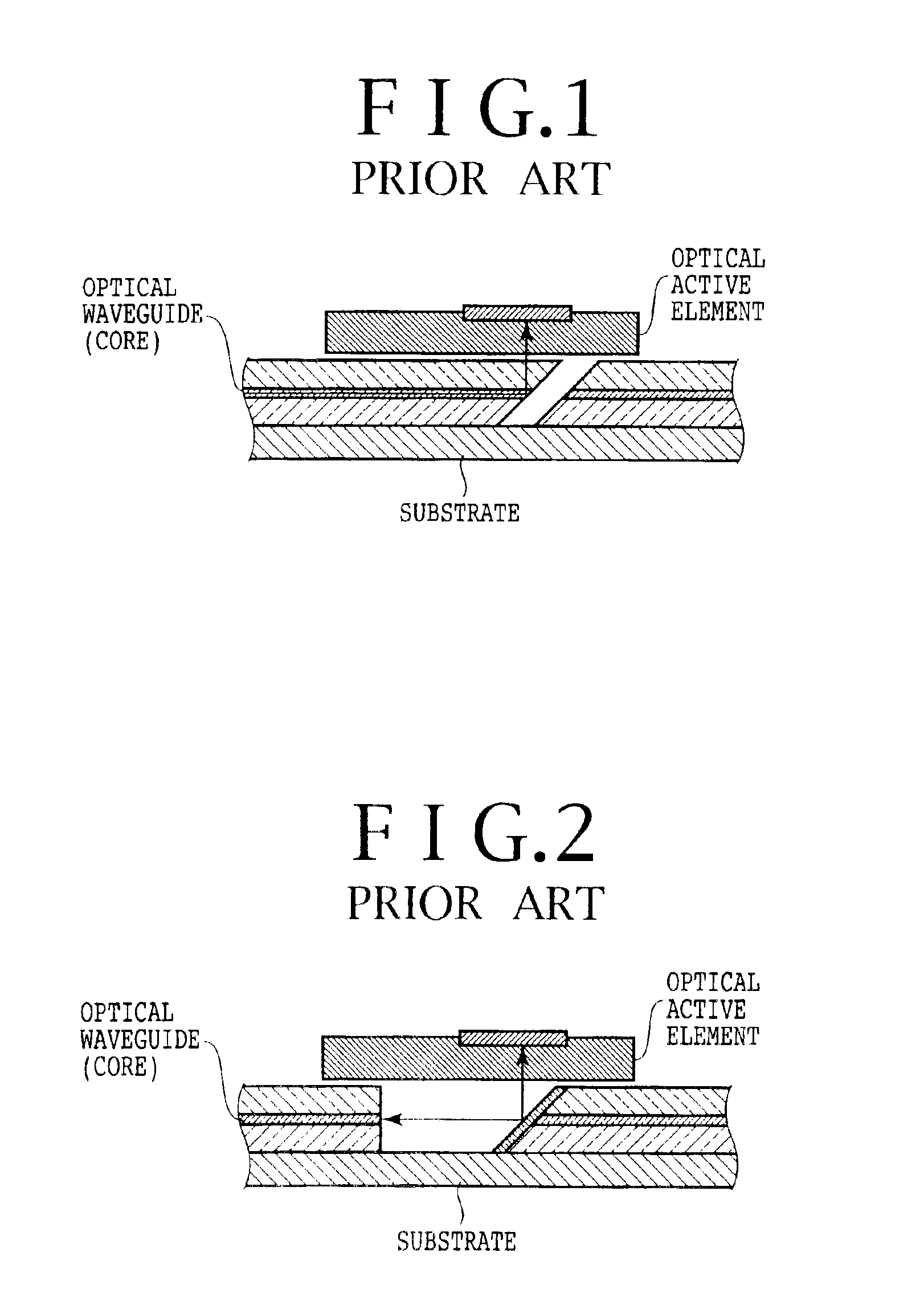
However, when the optical
integrated circuit becomes large in scale, the number of connection points to optical fibers or the like increases, so that the structure for
optical coupling between the optical
integrated circuit and the outside of the
package is complicated to cause an increase in cost.
Accordingly, the protective method using the hermetic
package sealing the whole of the optical
integrated circuit impairs the merit of the PLC type optical integrated circuit.
In the case of applying this method to the structure shown in FIG. 1, there is a problem that the sealing material such as resin may flow down along the inclined surface.
Accordingly, there is a substantial limit to the forming position of the inclined mirror, causing a great
disadvantage in designing the optical integrated circuit.
For example, in the case of forming the spatial reflection type structure by using separate components, there is a possibility that an
adhesive material for the separate components may expand because of variations in
operation temperature conditions or the like, causing a degradation in
optical coupling.
In general, it is difficult to form a mask for reprocessing a
wafer near a deep groove formed on the
wafer for forming the inclined surface.
If the end surface-to-inclined
surface distance is large, the reflection point of a
light beam on the inclined surface is largely deviated by the
refraction at the light emergent end surface, causing a limit to the
coupling tolerance between the end surface and the optical active element.
Further, since the separate component is used,
mass production and cost reduction are difficult.
According to the conventional forming method C, the fifth subject is difficult to satisfy.
According to the conventional forming method D, the third subject and the fourth subject are difficult to simultaneously satisfy, because these subjects are in a trade-off relation.
Thus, the subject on the end surface perpendicularity and the subject on the end surface-to-inclined
surface distance are in a trade-off relation, so that it is difficult for the conventional forming method D to simultaneously satisfy these two subjects.
In the forming method by inclined RIE, second RIE for the perpendicular end surface is required, so that simultaneous formation of the perpendicular end surface and the inclined surface is difficult.
Further, even when a
resist having a high
viscosity is applied by using a general spin coater, there may arise a problem that air bubbles present in the groove cannot be removed.
Thus, it is very difficult to realize the simultaneous formation of the perpendicular end surface and the inclined surface.
According to the conventional forming method F, the third subject and the fifth subject are difficult to simultaneously satisfy, because these two subjects are in a trade-off relation.
However, in the case of a thick film required for formation of the inclined surface (the film thickness being determined by the
etching selective ratio between the optical waveguide material and the
photomask material), the
linearity between the
exposure intensity and the amount of photoreaction in the direction along the depth is degraded to cause an increase in
exposure time.
Accordingly, near the top of the inclined surface where the amount of
exposure is desired to be reduced, the photoreaction of the
photomask proceeds in the direction along the depth, so that there is a high possibility of generation of pixel-sized unevenness.
However, in the case of increasing the heating speed in the heating process(post-baking) after development for a general
photomask material, not only a deterioration of a developed pattern due to
softening occurs, but also the photomask material over the perpendicular end surface is softened to cause a deterioration in perpendicularity of the mask.
Conversely, in the case of greatly decreasing the heating speed in the post-baking process, some kind of photomask material can be cured with the perpendicularity being maintained, but the smoothness of the inclined surface cannot be obtained.
Thus, in the forming method by the gray mask and RIE, it is difficult to simultaneously satisfy the subject on the perpendicularity of the end surface and the subject on the smoothness of the inclined surface because of the trade-off relation therebetween.
The conclusion drawn from the above discussion is that it is difficult to realize a spatial reflection type structure which can simultaneously satisfy all of the above subjects by any one of the above conventional forming methods.

