

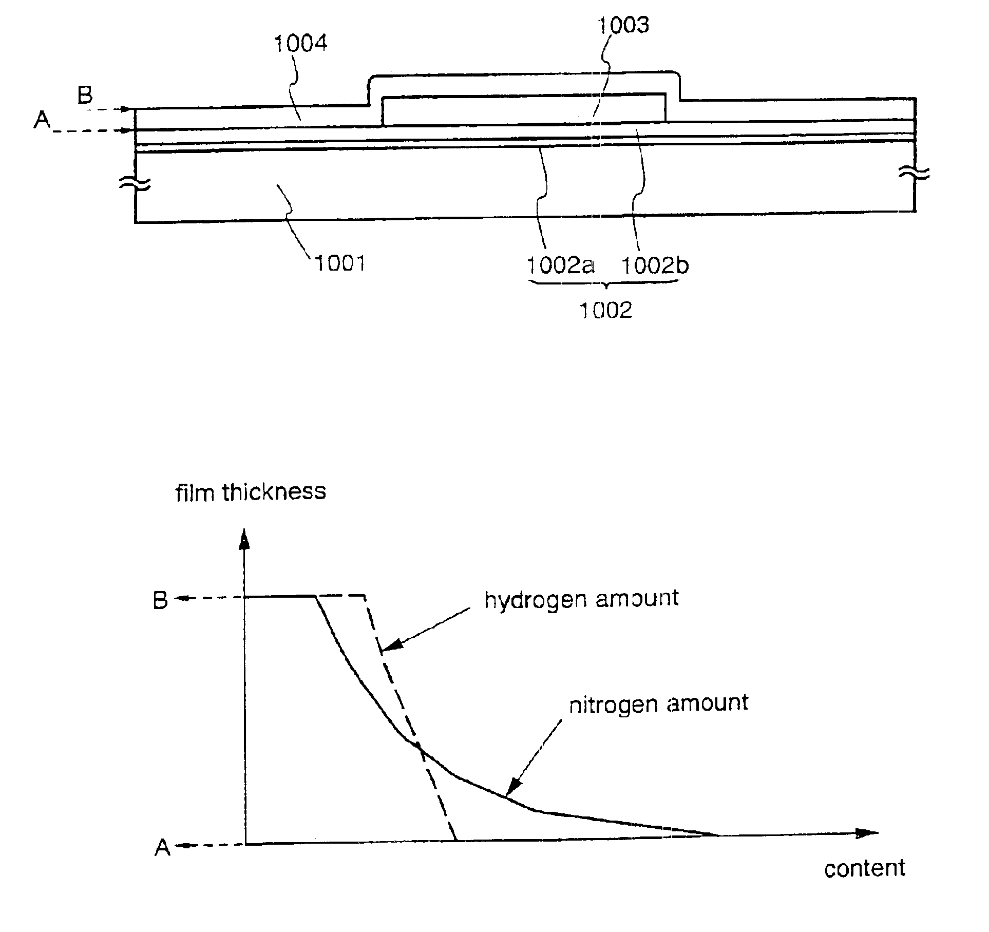
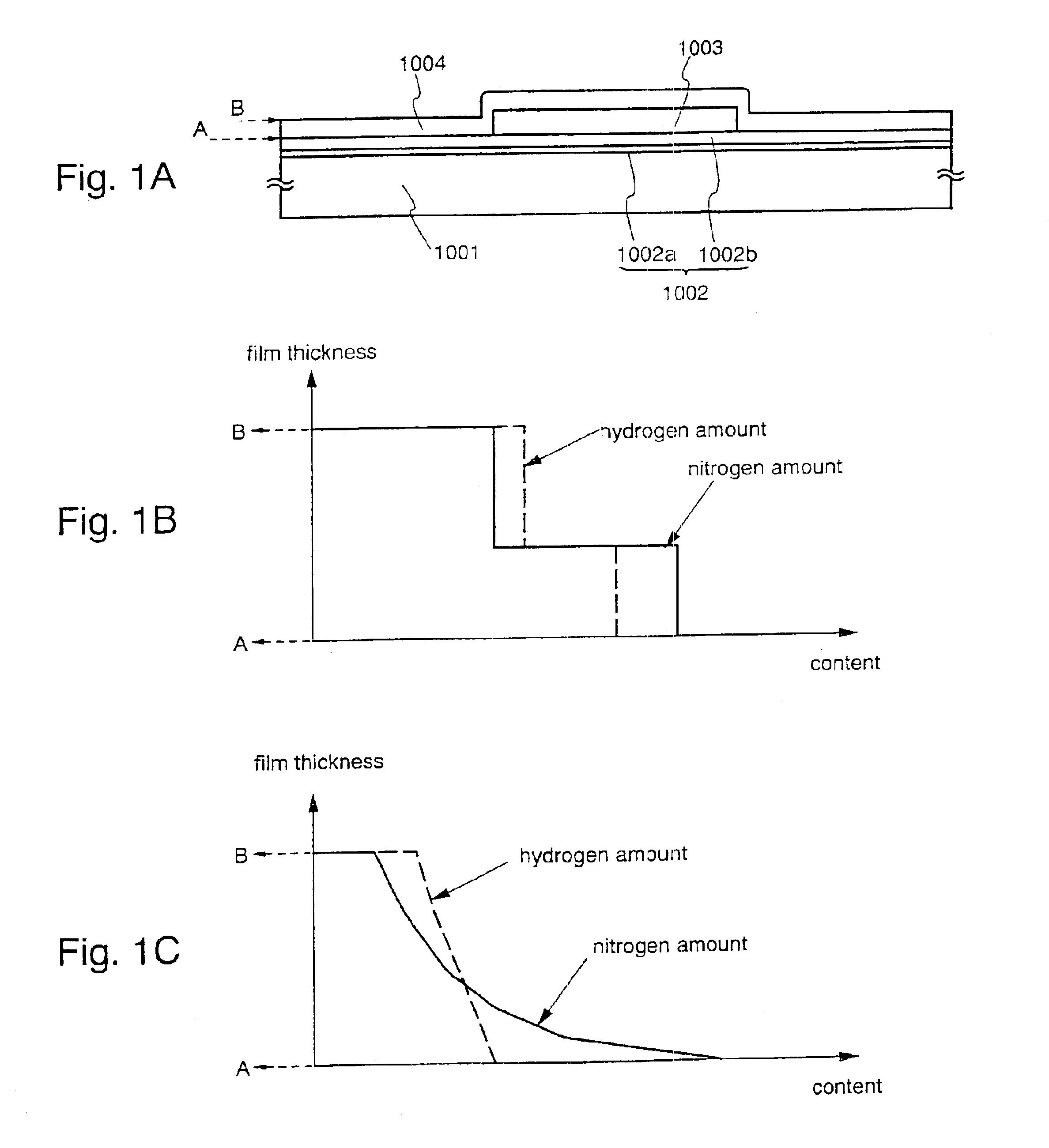
Method of fabricating a semiconductor device
a semiconductor device and manufacturing method technology, applied in semiconductor devices, instruments, electrical devices, etc., can solve the problems of slow deposition speed, inability to apply manufacturing process in view of circumstances, and becomes a factor for the increase of fabrication costs, and achieves small fluctuation width and higher stability
- Summary
- Abstract
- Description
- Claims
- Application Information
AI Technical Summary
Benefits of technology
Problems solved by technology
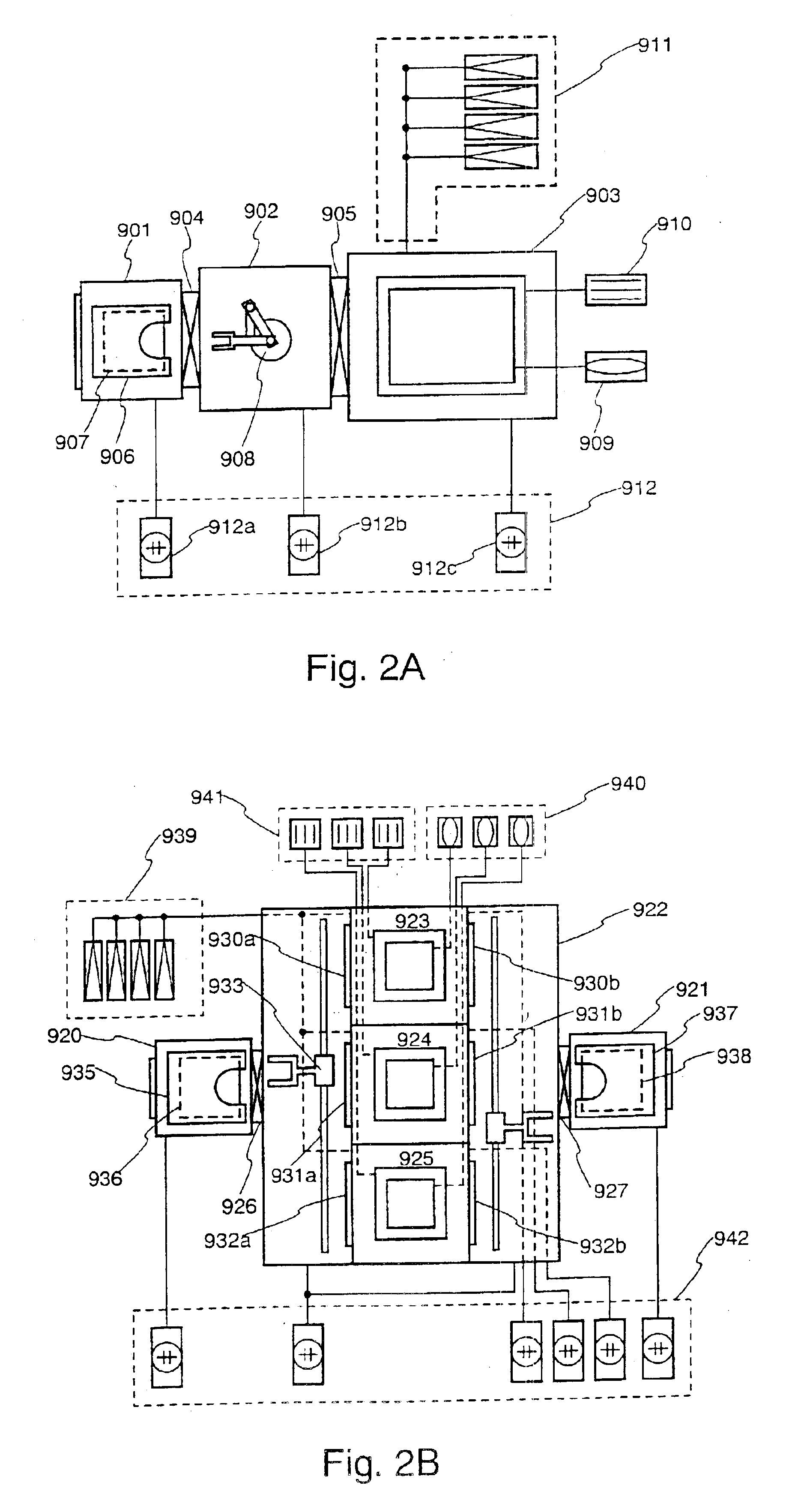
Method used
Image

Examples
embodiment 1
[Embodiment 1]
[0081]A method of manufacturing an n-channel TFT and a p-channel TFT, which is necessary for forming a CMOS circuit, on the same substrate is explained in Embodiment 1 in accordance with the process steps using FIGS. 3A to 4D.
[0082]A substrate such as a barium borosilicate glass substrate or alumino borosilicate glass substrate, typically Corning Corp. #7059 glass or #1737 glass substrate, is used for a substrate 101 in FIG. 3A. Alkaline metal elements such as sodium are contained in this type of glass substrate, although at trace amounts. This type of glass substrate shrinks by approximately several ppm to several tens of ppm due to the temperature during heat treatment, and therefore heat treatment may be performed in advance at a temperature on the order of 10 to 20° C. lower than the distortion point of the glass. A base film 102 is formed on the surface of the substrate 101 on which the TFT will be formed, in order to prevent contamination by alkaline metal elemen...
embodiment 2
[Embodiment 2]
[0107]This embodiment will be described with reference to FIG. 5A-FIG. 7D. A glass substrate (for example, substrate #1737 manufactured by Corning Incorporated) is employed as a substrate 601. First, gate electrodes 602 are formed on the substrate 601. In an example here, a tantalum (Ta) film was formed to a thickness of 200 nm by sputtering. Alternatively, each of the gate electrodes 602 may well be formed as a two-layer structure which consists of a tantalum nitride (TaN) film (50 nm thick) and a Ta film (250 nm thick). The Ta film is formed by sputtering with Ar gas and by employing Ta as a target. In this regard, when sputtering is performed with a mixed gas in which Xe gas is added to the Ar gas, the absolute value of an internal stress can be made 2×10⁸ Pa or less (FIG. 5A).
[0108]Subsequently, a gate insulating film 603 is formed. The gate insulating film 603 is endowed with a multi-layer structure which consists of a silicon oxynitride film (A) and a silicon oxy...
embodiment 3
[Embodiment 3]
[0123]In this embodiment, a method of simultaneously fabricating the pixel TFT and storage capacitor of a pixel unit and the TFTs of a driver circuit disposed outside the periphery of the pixel unit will be described in detail in accordance with the processing steps of the method.
[0124]Referring to FIG. 8A, a substrate 801 may be a glass substrate of barium borosilicate glass, alumino-borosilicate glass or the like, typified by Glass #7059 or Glass #1737 of Corning Incorporated, or a plastics substrate of plastics having no optical anisotropy, such as polyethylene terephthalate (PET), polyethylene naphthalate (PEN) or polyether sulfone (PES). In the case of employing the glass substrate, it may well be previously heat-treated at a temperature which is about 10° C.-20° C. lower than the strain point of the glass. On that surface of the substrate 801 over which the TFTs are to be formed, a base film 802 which includes an insulating film, such as silicon oxide film, silic...
PUM
| Property | Measurement | Unit |
|---|---|---|
| temperature | aaaaa | aaaaa |
| pressure | aaaaa | aaaaa |
| temperature | aaaaa | aaaaa |
Abstract
Description
Claims
Application Information