Multi-wavelength semiconductor lasers

a semiconductor laser and multi-wavelength technology, applied in the direction of semiconductor laser arrangement, semiconductor laser, laser, etc., can solve the problems of inability to integrate many wavelengths together, device is too long, complex focusing optics, etc., and achieves the effect of high reflectiveness and ease of fabrication and operation

Inactive Publication Date: 2005-08-30
NAT UNIV OF SINGAPORE
View PDF5 Cites 12 Cited by
  • Summary
  • Abstract
  • Description
  • Claims
  • Application Information

AI Technical Summary

Benefits of technology

[0011]The isolator section may be, for example, either a wavelength selective type or a light absorptive type. For the first type, it can be a distributed Bragg grating type isolator or a photonic bandgap crystal type isolator which is transmissive to one wavelength of the laser diode section but highly reflective to other wavelengths. For a dual wavelength laser source comprising two laser diode sections, an isolator

Problems solved by technology

However, many of the multiple wavelength laser sources or arrays fabricated rely on a large spatial separation between different wavelength elements, and therefore complex focusing optics are required to align the individual lasers to the optical fiber.
An inevitable drawback of this method is that there cannot be many wavelengths integrated togethe

Method used


Image

  • Multi-wavelength semiconductor lasers
  • Multi-wavelength semiconductor lasers
  • Multi-wavelength semiconductor lasers

Examples


Embodiment Construction

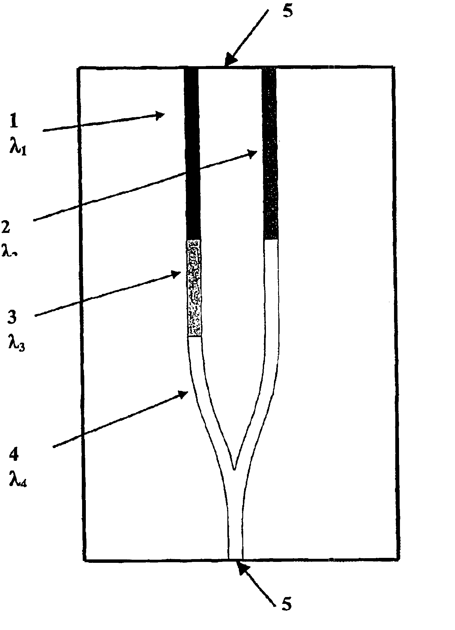
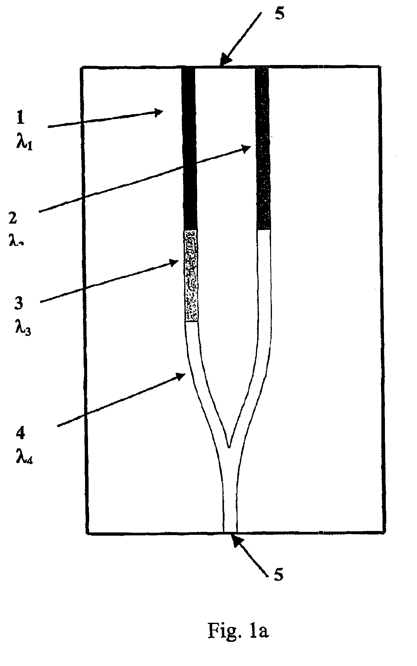
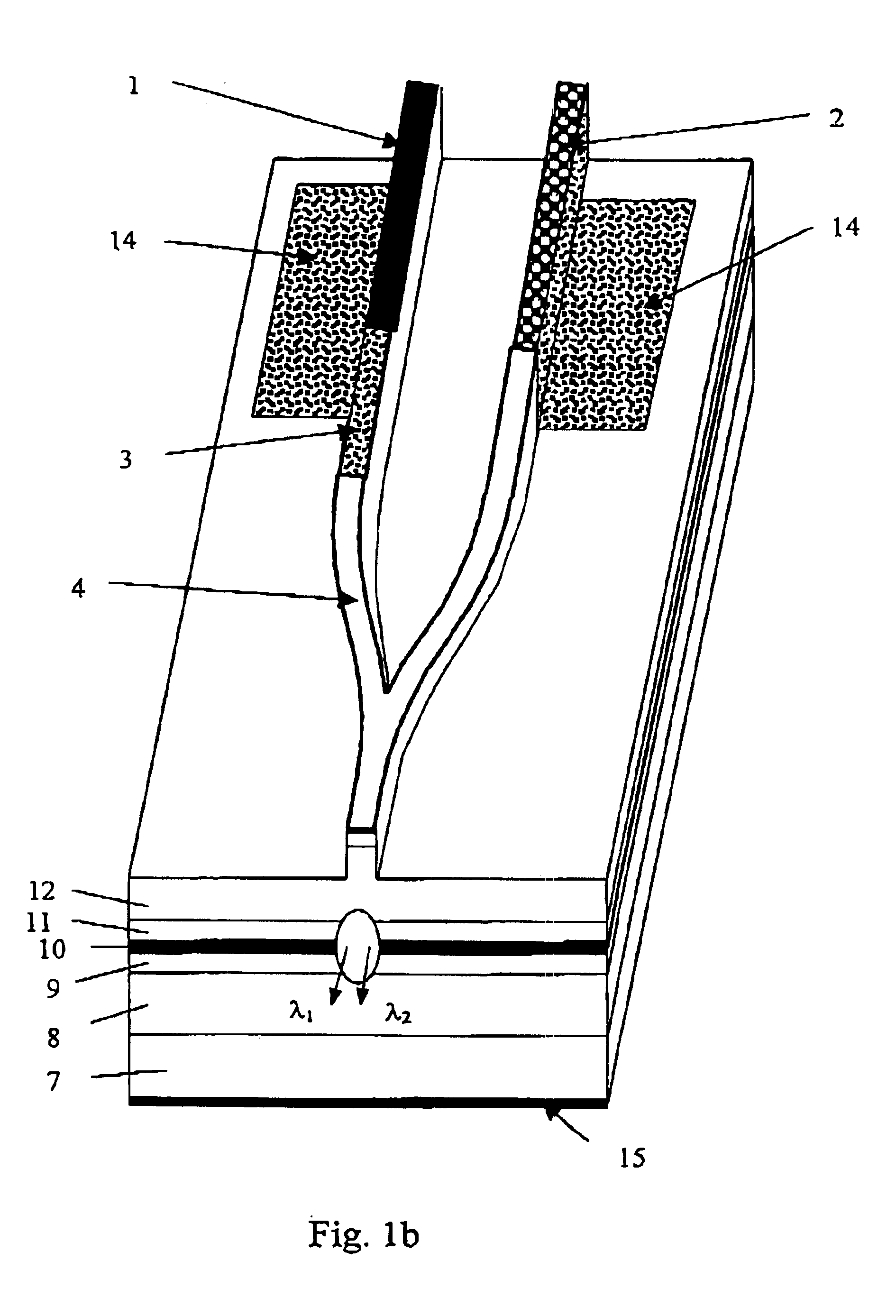
[0019]Referring to FIG. 1a, there is shown a schematic waveguide structure of a dual wavelength laser source monolithically integrated with an isolator and a Y-junction coupler. It contains laser diode sections 1 and 2, an isolator 3 and a Y-junction coupler 4. The structure includes cleaved laser facets 5.

[0020]The Y-junction coupler 4 is used to direct the two signals from the laser diode sections, (i.e. gain regions) 1 and 2 into a single output port. The length of the gain region and isolation region are 700 μm and 300 μm respectively. The Y-junction coupler 4 is composed of two S-bends with a radius of curvature of 1328 μm. The central space between the two branches is 34 μm. The bending loss in the Y-junction waveguide should be kept small in the design. FIG. 1b shows the schematic diagram of a ridge waveguide and vertical layer structure. The ridge waveguide can be formed by either wet chemical etching or Plasma dry etching (ICP or RIB). The wafer is a graded index separate c...


PUM


Abstract

A multi-wavelength semiconductor laser is formed by monolithically integrating a plurality of laser diodes (1, 2) with at least one isolator section (3) and a coupler (4), which couples the different emission wavelengths λ1, λ2 into one output port (5). The isolator section can be either a light absorptive type or wavelength selective type, including a Bragg grating type isolator or a photonic bandgap crystal type isolator. The coupler is preferably a Y-junction coupler, but can also be a multi-branch waveguide coupler or a waveguide directional coupler.

Description

FIELD OF THE INVENTION[0001]The present invention pertains to the field of semiconductor laser fabrication and in particular to a method for manufacturing integrated single output multiple wavelength lasers and related photonic integrated devices to be utilized in wavelength division multiplexing (WDM) optical communication system, optical recording and measurementBACKGROUND OF THE INVENTION[0002]Multi-wavelength laser sources are key elements for a variety of applications such as wavelength division multiplexing (WDM), optical recording, color displays and optical color printing. Several methods have been proposed and patented for the realization of these multi-wavelength laser sources and the integration with modulators, as can be seen in U.S. Pat. No. 4,955,030 (Menigaux), U.S. Pat. No. 4,831,629 (Paoli), U.S. Pat. No. 4,993,036 (Ikeda), U.S. Pat. No. 5,384,797 (Welch), U.S. Pat. No. 5,519,721 (Takano). They can be realized by the non-uniform current pumping resulting in areas wi...

Claims


Application Information

Patent Timeline
IPC IPC(8): H01S5/40H01S5/00H01S5/06H01S5/026
CPCH01S5/4068H01S5/0064H01S5/026H01S5/0265H01S5/0601H01S5/4087
Inventor CHUA, SOO JINTENG, JINHUA
Owner NAT UNIV OF SINGAPORE
Why Eureka
Try Eureka