Semiconductor module and mounting method for same

a technology of semiconductor modules and mounting methods, which is applied in the direction of semiconductor devices, semiconductor/solid-state device details, electrical apparatus, etc., can solve the problems of difficult transmission of heat generated in each chip to the wiring board, prone to cracking of the bonded end face between the stressed chip and the heat spread cap, and high cost, etc., to achieve high heat resistance and high reliability. , the effect of low cos

Inactive Publication Date: 2005-09-06
RENESAS ELECTRONICS CORP
View PDF34 Cites 23 Cited by
  • Summary
  • Abstract
  • Description
  • Claims
  • Application Information

AI Technical Summary

Benefits of technology

[0040]As the material for the wiring board, there may be used, for example, an organic printed wiring board containing a woven or non-woven fabric formed by glass fibers or organic fibers, a wiring tape such as a polyimide tape, or a ceramic substrate, according to the purpose for which the wiring board is to be used. An organic printed wiring board is suitable for a se

Problems solved by technology

First, in the multi-chip module described in U.S. Pat. No. 5,724,729, the stress exerted on a chip is not dispersed because there exists a gap between adjacent chips. Consequently, when a stress is applied to a certain chip, the bonded end face between the stressed chip and the heat spread cap is apt to be cracked. Moreover, since an underfill resin is not filled around the bump electrodes connecting the chips to the wiring board, the bump electrodes are apt to be oxidized, besides, heat generated in each chip is difficult to be transmitted to the wiring board.
Sho 63-29563, plural semiconductor devices are fixed to the heat spread plate mechanically through the heat transfer part, so if there are vari

Method used


Image

  • Semiconductor module and mounting method for same
  • Semiconductor module and mounting method for same
  • Semiconductor module and mounting method for same

Examples


embodiments 1

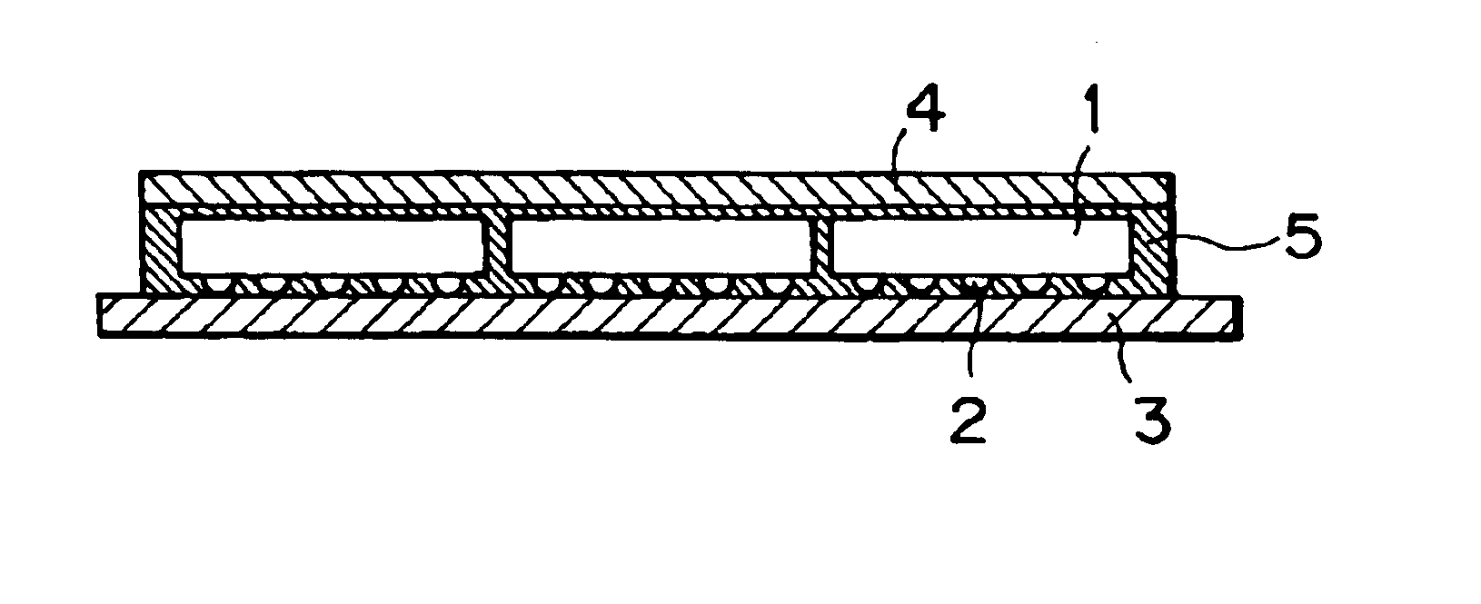
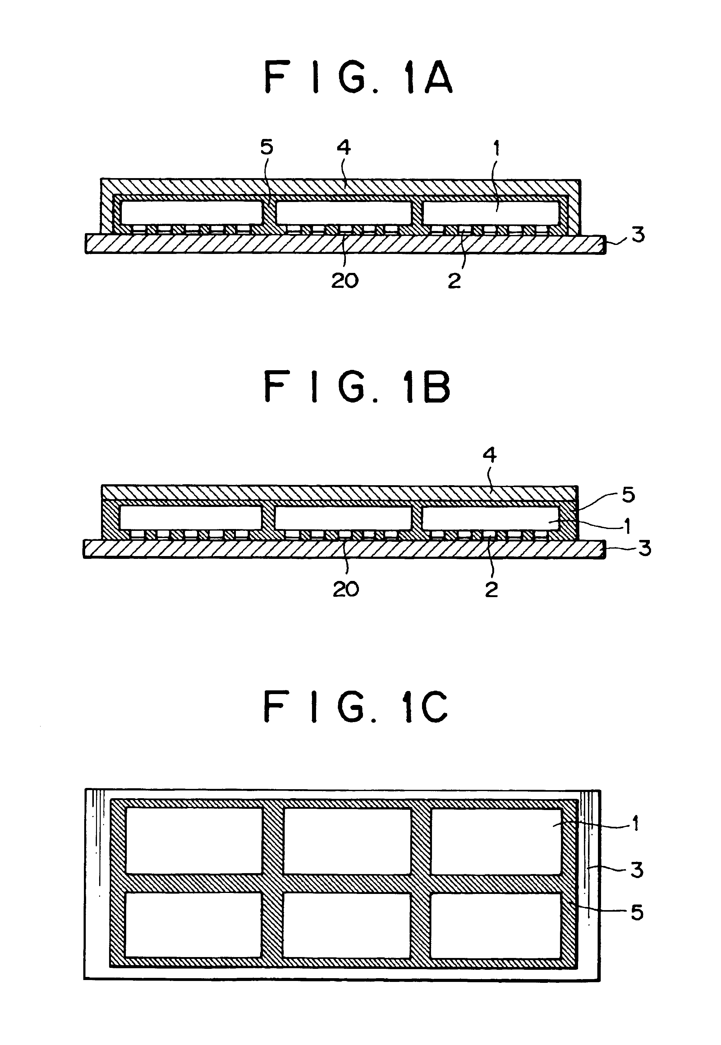
[0053]FIGS. 1A and 1B are sectional views of semiconductor modules wherein six semiconductor chips 1 are mounted on one side of a wiring board 3 with use of metal bumps 2, upper surfaces of the semiconductor chips are covered with a heat spread plate 4, and a resin composition 5 is filled between the wiring board and the heat spread plate. FIG. 1C is a top view without the heat spread plate.

[0054]In the module shown in FIG. 1A, both ends of the heat spread plate 4 are bent to afford a cap shape, with end faces of the cap being bonded to the wiring board. On the other hand, in the module shown in FIG. 1B, the heat spread plate is formed in a flat plate shape. A comparison of the two shows that the module illustrated in FIG. 1A is superior in point of heat spreading characteristic. The semiconductor chips 1 may be bare chips or may be semiconductor packages such as CSPs. Though not shown in the drawing, one end of the metal bumps 2 is electrically connected to pads of the bare chips a...

embodiments 2

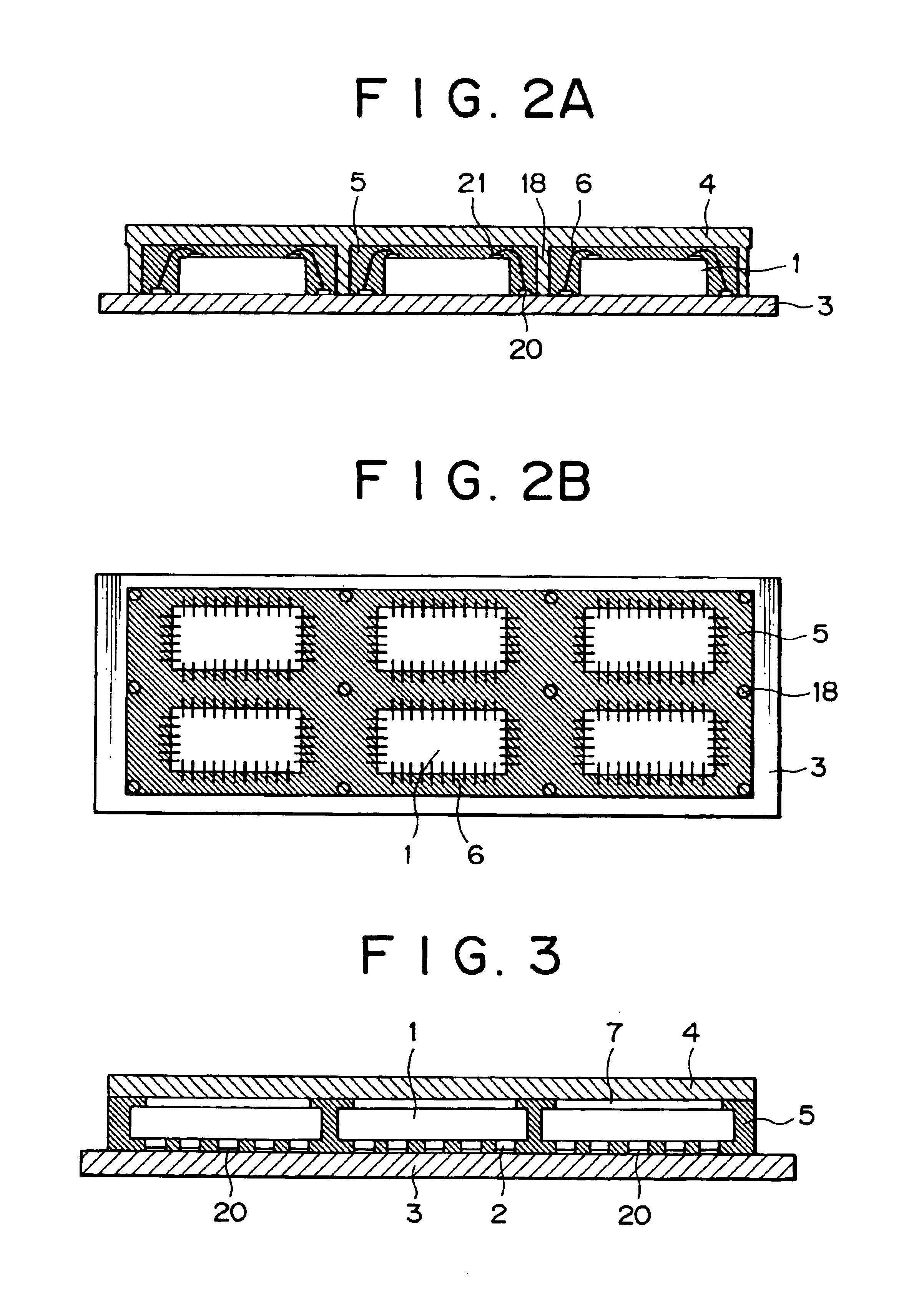
[0061]FIG. 2A is a sectional view of a semiconductor module wherein six semiconductor chips 1 are mounted on one side of a wiring board 3 by a metal wire bonding method and FIG. 2B is a top view thereof without a heat spread plate. The six semiconductor chips 1 are sealed by a resin composition 5 together with metal wires 6. A mounting method for this semiconductor module will be described below with reference to FIGS. 6A to 6F.

[0062]First, semiconductor chips 1 are mounted on a wiring board 3 with use of an insulative adhesive as in FIG. 6A. Preferably, the adhesive is an epoxy resin adhesive having a low elastic modulus which is 1 Gpa or lower at room temperature. Then, pads 21 formed on a circuit-formed side of each semiconductor chip 1 and pads 20 formed on the wiring board 3 are connected together using metal wires 6 as in FIG. 6B. Next, a resin composition 5 is put on each semiconductor chip as in FIG. 6C. Thereafter, as shown in FIG. 6D, a heat spread plate 4 is put on the re...

embodiment 3

[0065]FIG. 3 shows a semiconductor module wherein a plurality of semiconductor chips 1 are mounted on one side of a wiring board 3 with use of metal bumps 2. The semiconductor chips 1 and a heat spread plate 4 are bonded together using an adhesive 7, and a resin composition 5 is filled around the plural semiconductor chips. A mounting method for the semiconductor module of this structure will be described below with reference to FIGS. 7A to 7H.

[0066]First, as shown in FIG. 7A semiconductor chips 1 having metal bumps 2 and a wiring board 3 are provided. Next, as shown in FIG. 7B metal bumps 2 are connected to pads 20 formed on the wiring board 3. In FIGS. 7B et seq. the illustration of the pads 20 is omitted. Next, an adhesive superior in thermal conductivity is applied onto upper surfaces of the semiconductor chips 1 as in FIG. 7C. Preferably, the adhesive 7 is in the shape of a sheet. For this embodiment, an epoxy resin, a silicone resin, an acrylate or a methacrylate is suitable a...


PUM


Abstract

In a multi chip module of a structure wherein a plurality of bare or packaged semiconductor chips are mounted on a single wiring board and upper surfaces of the semiconductor chips are covered with a single heat spread plate, the whole space around the semiconductor chips thus sandwiched between the wiring board and the heat spread plate is filled with resin.
By so doing, the semiconductor chips are interconnected through the resin, so that even if a stress is exerted on any of the chips, it is dispersed and therefore it is possible to diminish the occurrence of cracks in the chips and the heat spread plate caused by stress concentration. Besides, since the semiconductor chips and the heat spread plate are bonded together with resin, even if there are variations in size of the chips, both can be bonded easily. Further, the bonding of all the chips and the heat spread plate can be done in a single process.

Description

[0001]This application is a divisional of application Ser. No. 10 / 302,986, filed Nov. 25, 2002 (now U.S. Pat. No. 6,784,541), which, in turn, is a continuation of application Ser. No. 09 / 463,431, filed Jan. 27, 2000 (now U.S. Pat. No. 6,627,997), which is the National Stage of International Application No. PCT / JP99 / 01558, filed Mar. 26, 1999, the entire disclosures of which are hereby incorporated by reference.TECHNICAL FIELD[0002]The present invention relates to a semiconductor module in which bare or packaged semiconductor chips are mounted on a wiring board, a heat spread plate is disposed above the semiconductor chips, and resin is filled around the semiconductor chips so that they are sandwiched between the wiring board and the heat spread plate, as well as a mounting method for the semiconductor module. Particularly, the invention is concerned with a multi-chip module with a plurality of semiconductor chips mounted on a single wiring board, as well as a mounting method for the...

Claims


Application Information

Patent Timeline
IPC IPC(8): H01L21/56H01L23/42H01L23/433H01L25/065
CPCH01L21/56H01L21/565H01L23/42H01L23/4334H01L25/0655H01L2224/48091H01L2224/48227H01L2224/49175H01L2224/73253H01L2924/0102H01L2924/16152H01L2924/16153H01L24/48H01L24/49H01L2924/01322H01L25/0652H01L2224/16225H01L2224/73265H01L2224/451H01L2224/45015H01L24/45H01L24/73H01L2924/181H01L2924/00014H01L2924/00H01L2224/32225H01L2924/00012H01L2924/20752
Inventor EGUCHI, SHUJINAGAI, AKIRAAKAHOSHI, HARUOUENO, TAKUMISATOH, TOSHIYAOGINO, MASAHIKONISHIMURA, ASAOANJO, ICHIROTANAKA, HIDEKI
Owner RENESAS ELECTRONICS CORP
Why Eureka
Try Eureka