Two step exposure to strengthen structure of polyimide or negative tone photosensitive material

a negative tone, polyimide technology, applied in the direction of photosensitive materials for photomechanical equipment, instruments, photomechanical treatment, etc., can solve the problems of reducing the height of the etch mask, difficult control, and etch selectivity, so as to reduce the amount of developer needed, reduce the amount of rework, and reduce the yield and reliability of the final device

Inactive Publication Date: 2005-09-13
TAIWAN SEMICON MFG CO LTD
View PDF9 Cites 19 Cited by
  • Summary
  • Abstract
  • Description
  • Claims
  • Application Information

AI Technical Summary

Benefits of technology

[0024]The advantage of the present invention is that film thickness loss in the retained film after the first exposure is minimized while scum in regions intended to be clear of photoresist or polyimide precursor is avoided. This greatly reduces the amount of developer needed per substrate and significantly lowers the amount of rework involving additional develop time to remove scum or stripping the photosensitive layer and repeating the coating and patterning process if scum cannot be developed away. The extra processing from rework in prior art can introduce defects that will lower the yield and reliability of the final device. Another benefit is that the retained film after the second exposure has a higher mechanica

Problems solved by technology

The wet etch process in the cited patent involves alternating the etchant and DI water treatments several times which is time consuming and can be difficult to control.
However, since the two layers are both composed of organic materials, the etch selectivity is poor and the height of the etch mask is decreased at about the same rate as the hole is formed in the polyimide layer.
Since polyamic esters tend to contain a large amount of aromatic groups which have a high optical absorbance below about 260 nm, their usefulness in 248 nm exposure methods is limited.
One drawback of this approach is that chemically amplified (CA)

Method used


Image

  • Two step exposure to strengthen structure of polyimide or negative tone photosensitive material
  • Two step exposure to strengthen structure of polyimide or negative tone photosensitive material
  • Two step exposure to strengthen structure of polyimide or negative tone photosensitive material

Examples


first embodiment

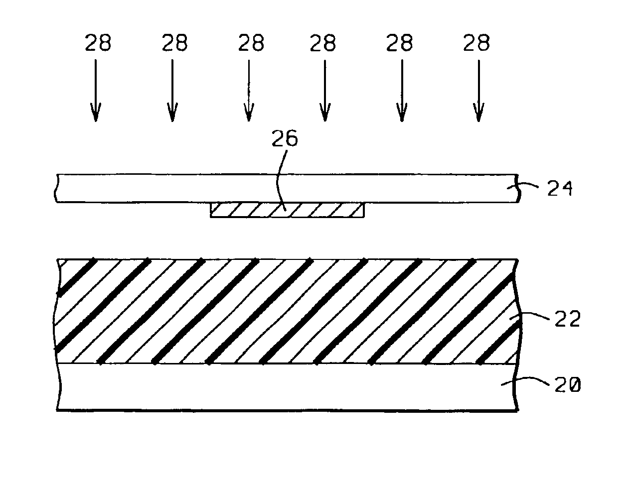
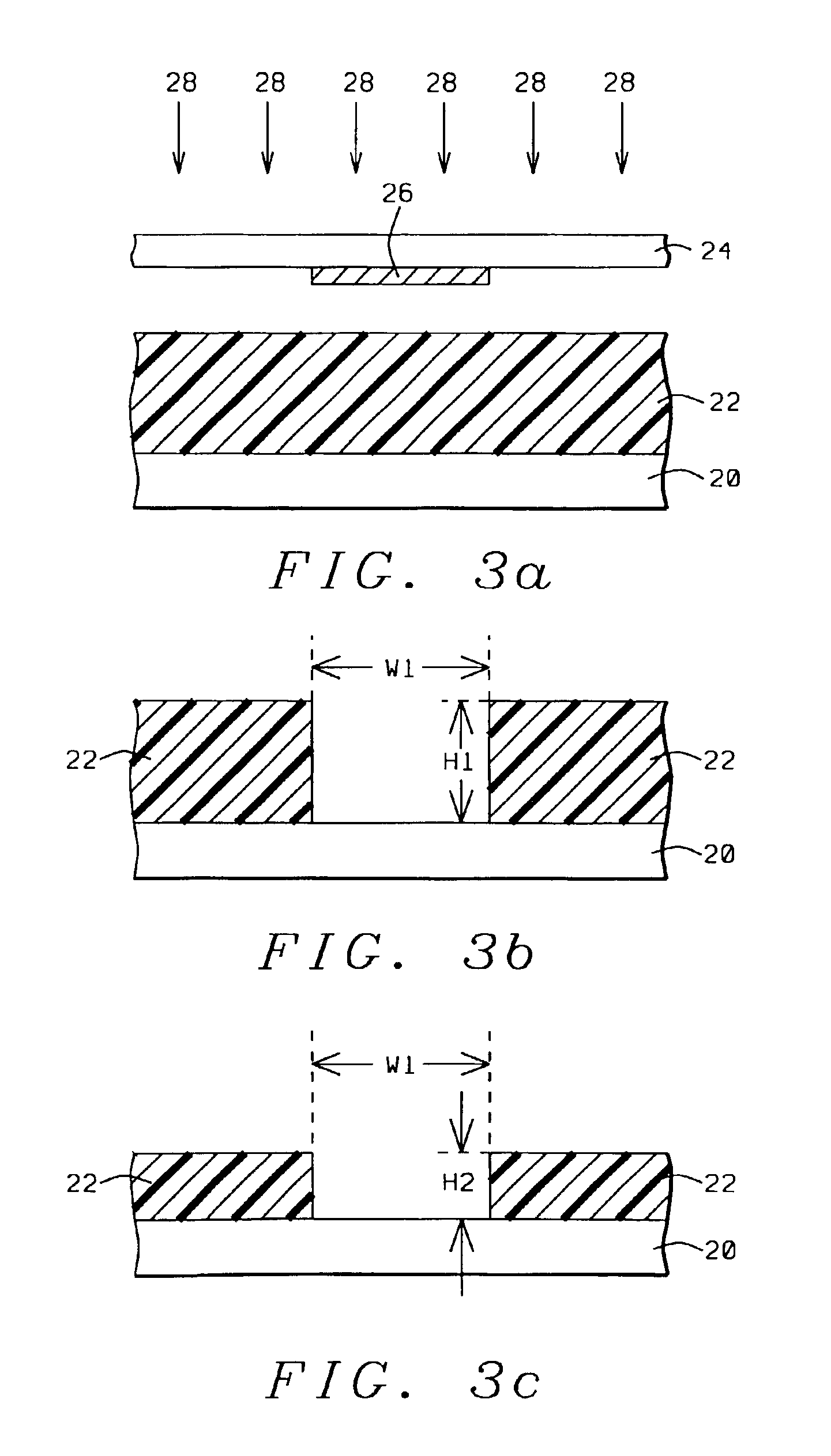
[0036]In the first embodiment as depicted in FIGS. 3a-3c, a substrate 20 is provided upon which a negative photosensitive polyimide precursor film 22 has been spin coated. The precursor material is typically a polyamic acid or polyamic ester. The thickness of film 22 can vary from a few microns to more than 10 microns and is preferably in a range of 8 to 10 microns after a low temperature bake that is, for example, about 100° C. for 5 minutes. Substrate 20 is silicon, ceramic or other appropriate materials that are common in semiconductor device manufacturing processes. Referring to FIG. 3a, a reticle or mask comprised of a transparent substrate 24 such as quartz and an opaque patterned coating 26 which is typically chrome or chromium is positioned between the exposure source 27 and the substrate 20. Radiation 28 from the exposure tool is blocked by opaque regions 26 on the mask and is transmitted through regions in quartz 24 which are not covered by chrome 26.

[0037]Exposure tools a...

second embodiment

[0048]In a second embodiment, the photosensitive composition is a negative tone photoresist formulation that is crosslinked by a free radical mechanism. Referring to FIG. 4a, the negative tone photoresist 44, hereafter referred to as negative resist, is spin coated on a polyimide precursor layer 42 that is on substrate 40. Negative resist 44 is patterned in the same manner as depicted in FIG. 3a with exposing radiation 28 from an exposure source and a mask comprised of a transparent substrate 24 and an opaque pattern 26. Layer 44 can be exposed with one or more wavelengths of radiation selected from a region extending from about 600 nm to about 300 nm including g-line (436 nm) and i-line (365 nm). Negative resist 44 is developed in an aqueous base solution to provide a pattern as shown in FIG. 4b with a space width W2 that can range from 1 or 2 microns to over 10 microns. Layer 44 can be several microns thick and is preferably 2 microns or less in thickness.

[0049]A second exposure d...

third embodiment

[0052]In a third embodiment, the photosensitive composition is a negative tone photoresist formulation that is crosslinked by a chemical amplification mechanism. Since a chemically amplified (CA) resist is sensitive to trace amounts of bases such as amines that are likely to be present in a polyimide layer, an intermediate layer is inserted between the cured polyimide and the negative resist. This embodiment provides a potentially smaller space width W3 than W1 or W2 afforded by the other embodiments because of the higher resolution of CA resists and the possibility of performing a pattern transfer with a more selective etch.

[0053]Referring to FIG. 5a, a cured polyimide layer 52 is provided on a substrate 50. A barrier layer 54 is then deposited by spin coating, a CVD method, or by sputtering. This layer primarily functions as a chemical barrier but is also useful as an etch stop or for its anti-reflective properties during patterning a photoresist above it. Suitable materials may b...


PUM


Abstract

A method is provided for forming features in a polyimide layer that is employed as an insulating layer or buffer layer during the fabrication of semiconductor devices or chip packaging structures. A pattern is formed in a photosensitive layer that has a high film retention after the development step and a crosslinked network that strengthens and stabilizes it for subsequent processing. The process involves exposing a negative tone photosensitive layer with a first exposure dose that is less than the normal dose used to image the material. The exposed layer is developed to provide a scum free substrate. A second exposure dose then strengthens the formed image by crosslinking unreacted components. First and second exposure doses are determined from a plot of film thickness loss vs. exposure energy. The method applies to photosensitive polyimide precursors as well as negative photoresists that are crosslinked by free radical or chemical amplification mechanisms.

Description

FIELD OF THE INVENTION[0001]The invention relates to a method of fabricating a semiconductor device or chip packaging structure. More particularly, the present invention relates to patterning polyimide precursors or negative tone photosensitive compositions and processing to provide patterns with high structural strength and low defects.BACKGROUND OF THE INVENTION[0002]Polyimides are often selected as permanent layers in the fabrication of semiconductor devices or in chip packaging structures because of their excellent thermal stability to greater than 350° C., low k dielectric constants, and good mechanical properties. A popular application is to employ them as a buffer layer to protect underlying circuits from damage during assembly or other types of handling operations. Typically, a polyamic acid or polyamic ester layer containing an (—NH—) group and a —CO2R group where R=H or an alkyl substituent as shown in FIG. 1 is patterned with exposing radiation and then cured to form a cy...

Claims


Application Information

Patent Timeline
IPC IPC(8): H01L21/02H01L21/302H01L21/31
CPCG03F7/11G03F7/2024H01L21/0274H01L21/31144G03F7/0382
Inventor LU, SHIN-RUNGLAN, HO-KU
Owner TAIWAN SEMICON MFG CO LTD
Why Eureka
Try Eureka