On chip heating for electrical trimming of polysilicon and polysilicon-silicon-germanium resistors and electrically programmable fuses for integrated circuits

Inactive Publication Date: 2005-10-25
TEXAS INSTR INC
View PDF7 Cites 36 Cited by
  • Summary
  • Abstract
  • Description
  • Claims
  • Application Information

AI Technical Summary

Benefits of technology

[0008]The electrical trimming of integrated circuit resistors and electrical programming of integrated circuit fuses according to the present invention is characterized by forming heating elements in close proximity to the resistor and fuse elements. By flowing current through the heating elements during the resistor trim cycle or fuse programming cycle the current required to trim the resistor or program the fuse is greatly reduced over existing devices. The efficiency of the present invention can be enhanced by forming a silicide film on the resistor and/or fuse element. In the present invention, the resistor, fuse, and heating structures can be formed using polysilicon, polysilicon-germanium, or other suitable silicon containing materials. The advantages of the present invention include providing a si

Problems solved by technology

High-speed precision analog and mixed-signal IC applications, (such as low offset voltage operational amplifiers, analog frequency tuning circuits, voltage controlled oscillators, and analog-to-digital (ADC) and digital-to-analog (DAC) converters) require high performance CMOS and BiCMOS technologies that are ultimately limited by the accuracy of both the active and passive components of the technology.
Although these techniques are highly accurate and easily reproducible, the electrical trim techniques require a high current electrical trim path to the resistor, which may be a severe limitation for many circuit applications.
Although this method works for some circuit applications, it is of limited use for many circuit applications that cannot have diode connected trim pads or cannot tolerate the high current densities required for trimming the resistors.
Be

Method used


Image

  • On chip heating for electrical trimming of polysilicon and polysilicon-silicon-germanium resistors and electrically programmable fuses for integrated circuits
  • On chip heating for electrical trimming of polysilicon and polysilicon-silicon-germanium resistors and electrically programmable fuses for integrated circuits
  • On chip heating for electrical trimming of polysilicon and polysilicon-silicon-germanium resistors and electrically programmable fuses for integrated circuits

Examples


Embodiment Construction

[0017]The invention will be described with reference to FIGS. 2-6. It comprises an on chip heater for resistor trimming and fuse programming.

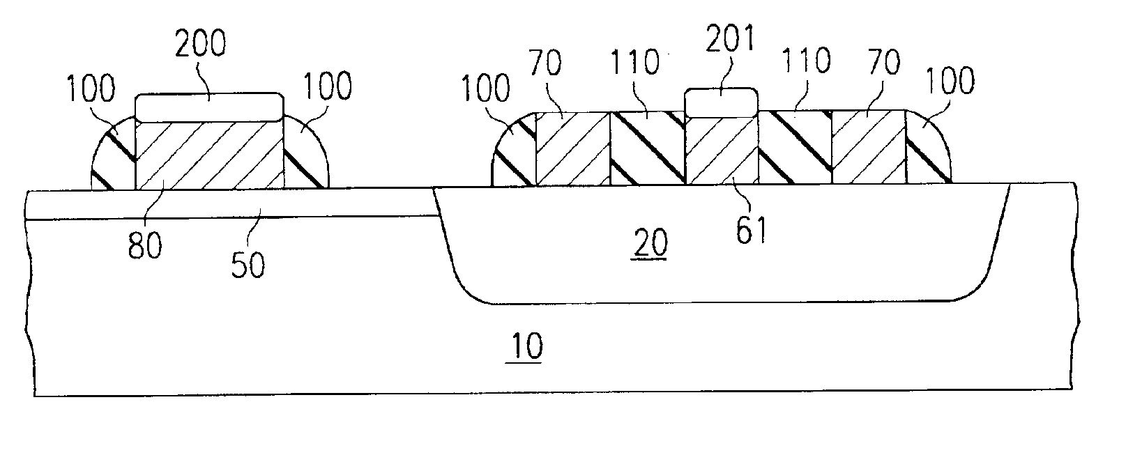
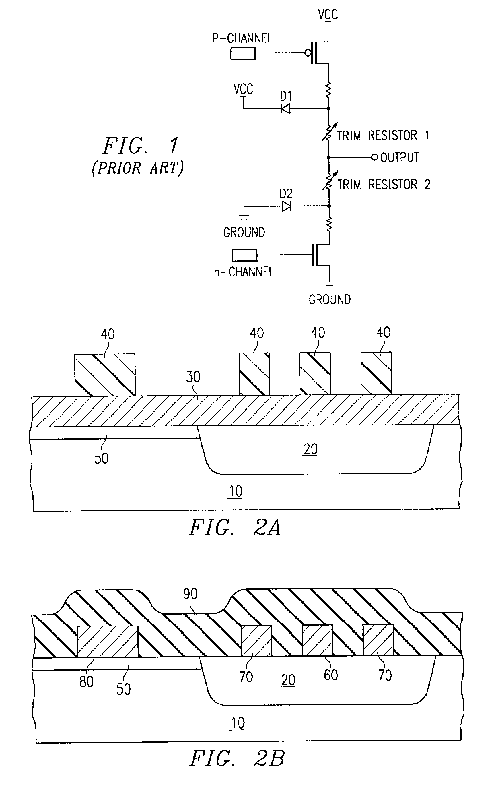
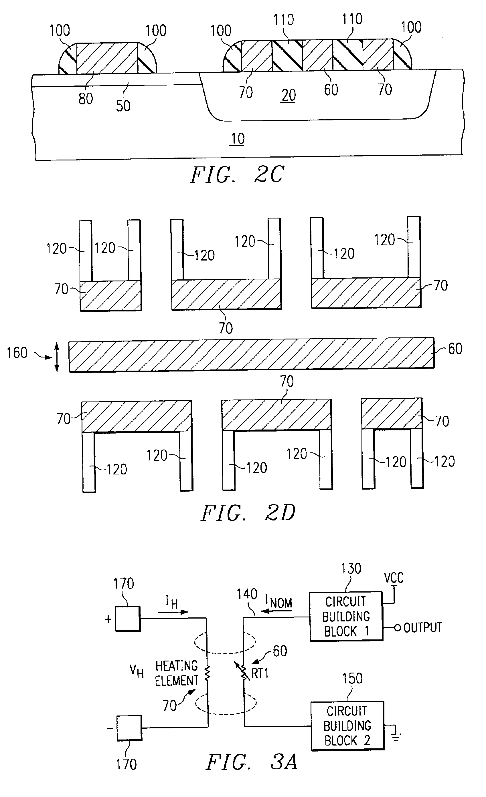
[0018]Shown in FIGS. 2A-2D is an embodiment of the instant invention. As shown in FIG. 2A, isolation structures 20 are formed in a substrate wafer 10. The substrate wafer 10 can be a bulk silicon wafer, a silicon wafer with an epitaxial layer, or a silicon-on-insulator (SOI) wafer. An SOI wafer would have a buried insulator layer which is not shown in the Figures for clarity. The isolation structures can be shallow trench isolation (STI) structures or local oxidation (LOCOS) structures. Each of these STI or LOCOS structures can be formed using standard CMOS processing technology. A gate dielectric layer 50 is formed in those regions of the substrate 10 where CMOS circuits will be fabricated. This gate dielectric layer can be an oxide, an oxynitride, a silicate, or any combination of these materials. Following the formation of the gate dielectri...


PUM


Abstract

An integrated circuit programmable structure (60) is formed for use a trim resistor and/or a programmable fuse. The programmable structure comprises placing heating elements (70) in close proximity to the programmable structure (60) to heat the programmable structure (60) during programming.

Description

[0001]This application claims priority under 35 USC § 119(e)(1) of provisional application Ser. No. 60 / 232,926, filed Sep. 15, 2000.FIELD OF THE INVENTION[0002]The present invention relates to an on chip heating device and method for use in trimming polysilicon and polysilicon-silicon-germanium resistors and for heat augmented electrical programming of fuses for integrated circuits.BACKGROUND OF THE INVENTION[0003]High-speed precision analog and mixed-signal IC applications, (such as low offset voltage operational amplifiers, analog frequency tuning circuits, voltage controlled oscillators, and analog-to-digital (ADC) and digital-to-analog (DAC) converters) require high performance CMOS and BiCMOS technologies that are ultimately limited by the accuracy of both the active and passive components of the technology. Inaccuracies and variations in thin film and thick film resistor deposition typically result in 10% to 20% variation from the designed resistor values, while the best case ...

Claims


Application Information

Patent Timeline
IPC IPC(8): H01C17/26H01C7/13H01C17/22H01L23/34H01L27/08
CPCH01C7/13H01C17/267H01L23/345H01L27/0802H01L2924/0002H01L2924/00
Inventor BABCOCK, JEFFREY A.PINTO, ANGELOHOWARD, GREGORY E.STEINMANN, PHILIPPBALSTER, SCOTT
Owner TEXAS INSTR INC
Why Eureka
Try Eureka