Anti-reflective coating composition with improved spin bowl compatibility

a technology of anti-reflective coating and spin bowl, which is applied in the direction of polyether coating, nuclear engineering, electrical equipment, etc., can solve the problems of reducing the resolution of the photoresist, affecting the shelf life of the photoresist, and affecting the image quality of the processed photoresist, so as to achieve the effect of prolonging the shelf li

Inactive Publication Date: 2005-11-08
BREWER SCI
View PDF6 Cites 23 Cited by
  • Summary
  • Abstract
  • Description
  • Claims
  • Application Information

AI Technical Summary

Benefits of technology

[0024]Finally, when the inventive anti-reflective coating compositions are subjected to a spin bowl compatibility test as defined in Example 5, they will achieve a result of at least about 90%, and preferably at least about 95%. It will be appreciated that this results in an effective anti-reflective coating composition that will not crosslink prematurely (e.g., such as in the spin bowl or drain pipes) and has a longer shelf life (won't crosslink during storage), but will substantially or completely crosslink during the bake stage.

Problems solved by technology

However, a frequent problem encountered by photoresists during the manufacturing of semiconductor devices is that activating radiation is reflected back into the photoresist by the substrate on which it is supported.
Such reflectivity tends to cause blurred patterns which degrade the resolution of the photoresist.
Degradation of the image in the processed photoresist is particularly problematic when the substrate is highly reflective.
One problem encountered with many prior art anti-reflective coating formulations is that they commonly use a thermal crosslinking system to yield a polymer-containing film which is insoluble in common photoresist solvents.
The use of such strong acid catalysts in an anti-reflective coating formulation creates processing problems.
This problem is known as spin bowl incompatibility.
Since spin coating has long been the industry accepted method of coating anti-reflective coatings and photoresists onto wafers, spin bowl incompatibility causes significant process interruptions and down time for wafer processing facilities.
This prevents waste material flow and may result in a small pool of waste photoresist collecting in the bottom of the spinner.
Since the crosslinked anti-reflective coating cannot be dissolved with solvents, the spinner must be disassembled to clear the drain, thus adding additional time and expense to the process.
Spin bowl incompatibility also causes the crosslinked anti-reflective coating to deposit on the sides of the spin bowl.
Eventually such build-up will be sufficiently present that it will interfere with wafer processing.
Again, because the crosslinked anti-reflective coating material cannot be cleaned with solvents, it may be necessary to replace the contaminated spin bowl with a new one.
It will be appreciated that this is both time-consuming and costly.
Furthermore, because most wafer processing facilities use automated, track-type systems, replacing spin bowls and cleaning drain pipes stop the track and results in downtime for an entire processing operation.

Method used


Image

  • Anti-reflective coating composition with improved spin bowl compatibility
  • Anti-reflective coating composition with improved spin bowl compatibility
  • Anti-reflective coating composition with improved spin bowl compatibility

Examples


example 1

Comparative Example (Control)

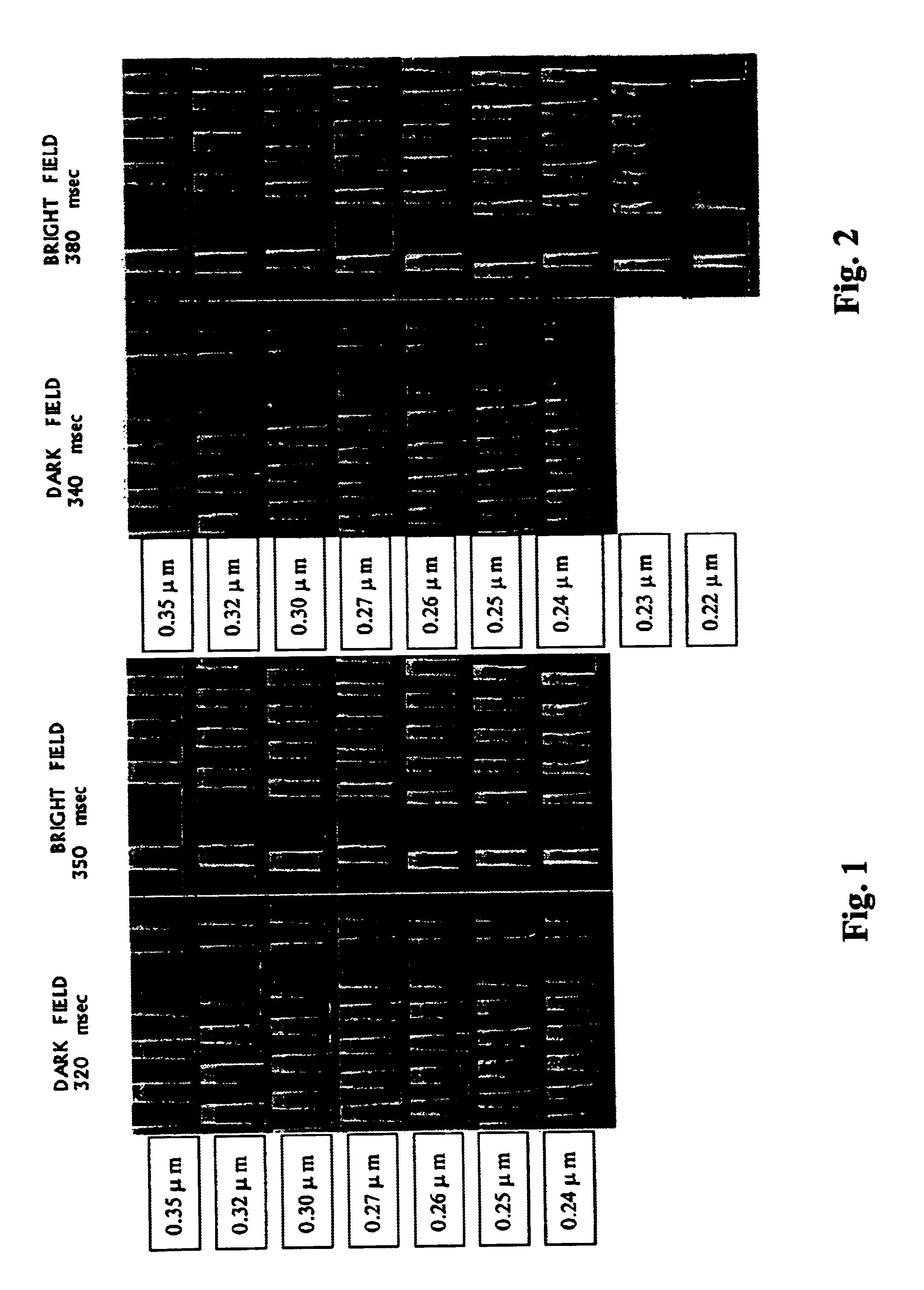
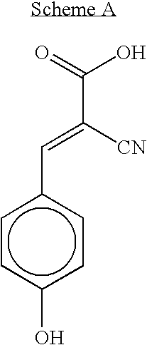
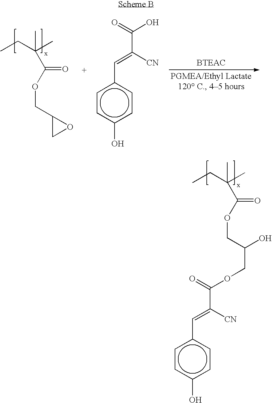
[0028]An anti-reflective coating was prepared according to prior art procedures in order to provide a control standard for spin bowl compatibility tests. A mixture containing the following ingredients was prepared: 11.60% by weight polymer solids (50% by weight benzyl methacrylate and 50% by weight hydroxypropyl methacrylate); 0.58% by weight of Powderlink® 1174 (a crosslinking agent obtained from Cytec); 0.1% by weight p-toluenesulfonic acid (pTSA); 9.69% by weight propylene glycol monomethyl ether acetate (PGMEA); 77.96% by weight propylene glycol monomethyl ether (PGME); and 0.07% by weight surfactant (FC-171, obtained from 3M). The mixture was stirred for one hour to yield a clear solution followed by ion exchange with 650C beads. The formulation was then filtered through a 1×0.2 μm absolute filter and a 2×0.1 μm absolute filter. The filtered material was spincoated onto a silicon wafer at a speed of 2500 rpm for 60 seconds followed by baking at 175°...

example 2

Preparation of an Anti-Reflective Coating According to the Invention

[0029]A mixture of the following ingredients was prepared: 11.60% by weight polymer solids (50% benzyl methacrylate and 50% hydroxypropyl methacrylate); 0.58% by weight Powderlink 1174; 0.075% by weight Bisphenol S (obtained from Aldrich); 0.025% by weight pTSA; 9.69% by weight PGMEA; 77.96% PGME; and 0.07% by weight FC-171 surfactant. The mixture was stirred for one hour to yield a clear solution followed by ion exchange with 650C beads. The formulation was then filtered through a 1×0.2 μm absolute filter and a 2×0.1 μm absolute filter. The filtered formulation was spincoated onto a silicon wafer at a speed of 2500 rpm for 60 seconds followed by baking at 175° C. for one minute. The resulting anti-reflective film had a thickness of about 880 Å. The absorbance of the film was as follows: about 13.66 / μm at a wavelength of 193 nm; about 0.54 / μm at a wavelength of 248 nm; and about 0.10 / μm at a wavelength of about 365 ...

example 3

Preparation of an Anti-Reflective Coating According to the Invention

[0030]An anti-reflective coating was prepared following the procedure described above in Example 2, but with 0.1% by weight Bisphenol S being used in place of 0.075% by weight Bisphenol S and 0.025% by weight pTSA.


PUM

PropertyMeasurementUnit
temperatureaaaaaaaaaa
pKaaaaaaaaaaa

Abstract

Anti-reflective compositions and methods of using those compositions to form circuits are provided. The compositions comprise a polymer dissolved or dispersed in a solvent system. In one embodiment, the compositions comprise less than about 0.3% by weight of a strong acid. In another embodiment, the weight ratio of strong acid to weak acid in the composition is from about 0:100 to about 25:75. Examples of preferred weak acid compounds include phenolic compounds (e.g., Bisphenol S, Bisphenol A, α-cyano-4-hydroxycinnamic acid), carboxylic acids (e.g., acetic acid), phosphoric acid, and cyano compounds. The polymer and other ingredients are preferably physically mixed in a solvent system. The resulting compositions are spin bowl compatible (i.e., they do not crosslink prior to the bake stages of the microlithographic processes or during storage at room temperature).

Description

RELATED APPLICATIONS[0001]This application is a continuation application of U.S. patent application Ser. No. 09 / 836,832, filed Apr. 17, 2001, now abandoned incorporated by reference herein.BACKGROUND OF THE INVENTION[0002]1. Field of the Invention[0003]The present invention is concerned with new anti-reflective compositions for use in the manufacture of microelectronic devices. These compositions include little or no strong acids so that premature crosslinking (e.g., such as during storage) is minimized or prevented.[0004]2. Description of the Prior Art[0005]Integrated circuit manufacturers are consistently seeking to maximize substrate wafer sizes and minimize device feature dimensions in order to improve yield, reduce unit case, and increase on-chip computing power. Device feature sizes on silicon or other chips are now submicron in size with the advent of advanced deep ultraviolet (DUV) and i-line microlithographic processes.[0006]However, a frequent problem encountered by photor...

Claims


Application Information

Patent Timeline
Patent Type & Authority Patents(United States)
IPC IPC(8): C08J3/24G03F7/09G03F7/11B32B7/02C09D5/00C09D7/12C09D105/00C09D133/00C09D161/20C09D163/00C09D167/00C09D171/00C09D179/08C09D201/00G03F7/004H01L21/027
CPCC08J3/241G03F7/091Y10S430/151
Inventor SHAO, XIEMEADOR, JIM D.BHAVE, MANDARKRISHNAMURTHY, VANDANANOWAK, KELLY A.FOWLER, MICHELLEDESHPANDE, SHREERAM V.
Owner BREWER SCI
Why Eureka
Try Eureka