Laser beam machining method for wiring board, laser beam machining apparatus for wiring board, and carbonic acid gas laser oscillator for machining wiring board

a laser and wiring board technology, applied in the direction of lithographic masks, manufacturing tools, etching metal masks, etc., can solve the problems of requiring a considerable machining time, simultaneously machine adjacent positions, poor productivity, etc., and achieve the effect of rapid and accurate machined and improved productivity

Inactive Publication Date: 2005-12-06
MITSUBISHI ELECTRIC CORP
View PDF29 Cites 19 Cited by
  • Summary
  • Abstract
  • Description
  • Claims
  • Application Information

AI Technical Summary

Benefits of technology

[0018]In order to overcome the above problems, it is an object of the present invention to provide a stable laser beam machining method for a wiring board, in which a printed board with an insulating base material containing cloth-like glass fibers can rapidly and accurately be machined, for example, drilled for a through-hole, an inner via hole and a blind via hole, grooved, or cut for an outside shape without roughness of a machined portion and the need for complicated after-treatment of additional deposit, and no damage is caused to copper foil. It is also an object of the present invention to provide a laser beam machining apparatus for a wiring board, for realizing the laser beam machining method for the wiring board and improving productivity.
[0019]It is another object of the present invention to provide a carbonic acid gas laser oscillator for machining a wiring board, which can output a laser beam with a pulse width most suitable for the laser beam machining method for the wiring board.

Problems solved by technology

However, the method has drawbacks in that the finer hole diameter is limited, for example, drilling for a hole diameter of φ0.2 mm or less is very difficult to cause heavy wear of the drill such as breakage, resulting in poor productivity due to a long time required for replacement of the drill.
Further, it is difficult to simultaneously machine adjacent positions, thereby requiring a considerable machining time.
Since it is difficult to control a hole depth in the drill machining with accuracy of 0.1 mm or less, it is difficult to form a blind via hole in such a thin-walled insulating base material.
However, the mechanical methods such as router machining are unpractical since the above limitation is similarly imposed thereon.
In this case, there are problems in that metallic deposit for conduction can not easily be coated on a hole inner wall due to the extremely rough inner wall of the hole, and reliability of the metallic deposit can not be ensured.
The problems are generated because the insulating material of the printed board is not only the composite material made of organic material and inorganic material but also heterogeneous material in which the organic material and the inorganic material are contained in clusters to some extent.
Further, there is another problem in that a uniform machined hole can not be provided due to differences in, for example, absorption coefficient of the laser beam, decomposition temperature, and thermal diffusivity between an organic material portion and an inorganic material portion.
For example, since a wavelength of the laser beam in the eximer laser can not easily be absorbed by the glass, sufficient energy for decomposition of the glass can not be supplied so that a glass portion is difficult to remove, resulting in a problem of a rough machined hole.
However, when energy density of 20 J / cm2 required to efficiently machine glass epoxy material is obtained in the TEA-carbonic acid gas laser, excessively high power density of 2×10⁷ W / cm2 or more is caused due to the narrow pulse width of 1 μs or less.
Such high power density may easily cause plasma at the machined portion.
Once the plasma is formed, laser energy is absorbed by the plasma, resulting in insufficient energy reaching the machined portion.
Hence, it is difficult to remove glass having a high decomposition temperature, thereby causing a problem of the rough machined hole.
If the energy density is set to cause no plasma, the machining progresses extremely slowly, resulting in a problem of a reduction in productivity.
As a result, after the machining, the machined portion is coated with additionally deposited soot, thereby reducing reliability of insulation and reliability of metallic deposit in the printed board.
Hence, there is another problem of the need for the step of, for example, complicated after-treatment such as wet etching.
That is, there is in theory a problem of pulse response sensitivity at a time of pulse oscillation, in particular, a characteristic in which a time is required for a fall of a laser pulse.
Thus, the machining by the conventional carbonic acid gas laser having such a characteristic results in irradiation of the machined portion with a laser beam for a longer time, thereby causing a gradual temperature gradient around the machined portion.
When only the resin is excessively removed, there are problems in that projection of the glass fibers results in a rough machined hole as shown in FIG. 35, and the long heating time generates a char layer on a wall surface of the hole.
Further, carbides are generated around the machined portion, and the laser beam is absorbed by the copper through the carbides, resulting in frequent damage to the copper foil as shown in FIG. 36.
Hence, there is a problem in that the blind via hole is difficult to form in the above laser beam machining methods.
Though descriptions have been given of the machining for the hole, the same problems are caused in the grooving and the cutting.

Method used


Image

  • Laser beam machining method for wiring board, laser beam machining apparatus for wiring board, and carbonic acid gas laser oscillator for machining wiring board
  • Laser beam machining method for wiring board, laser beam machining apparatus for wiring board, and carbonic acid gas laser oscillator for machining wiring board
  • Laser beam machining method for wiring board, laser beam machining apparatus for wiring board, and carbonic acid gas laser oscillator for machining wiring board

Examples


embodiment 1

[0075

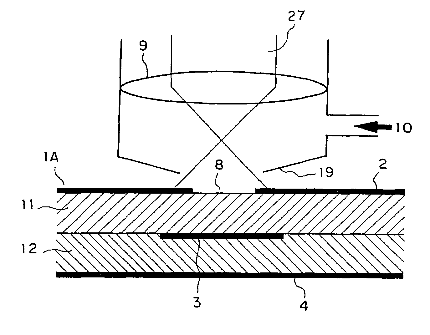
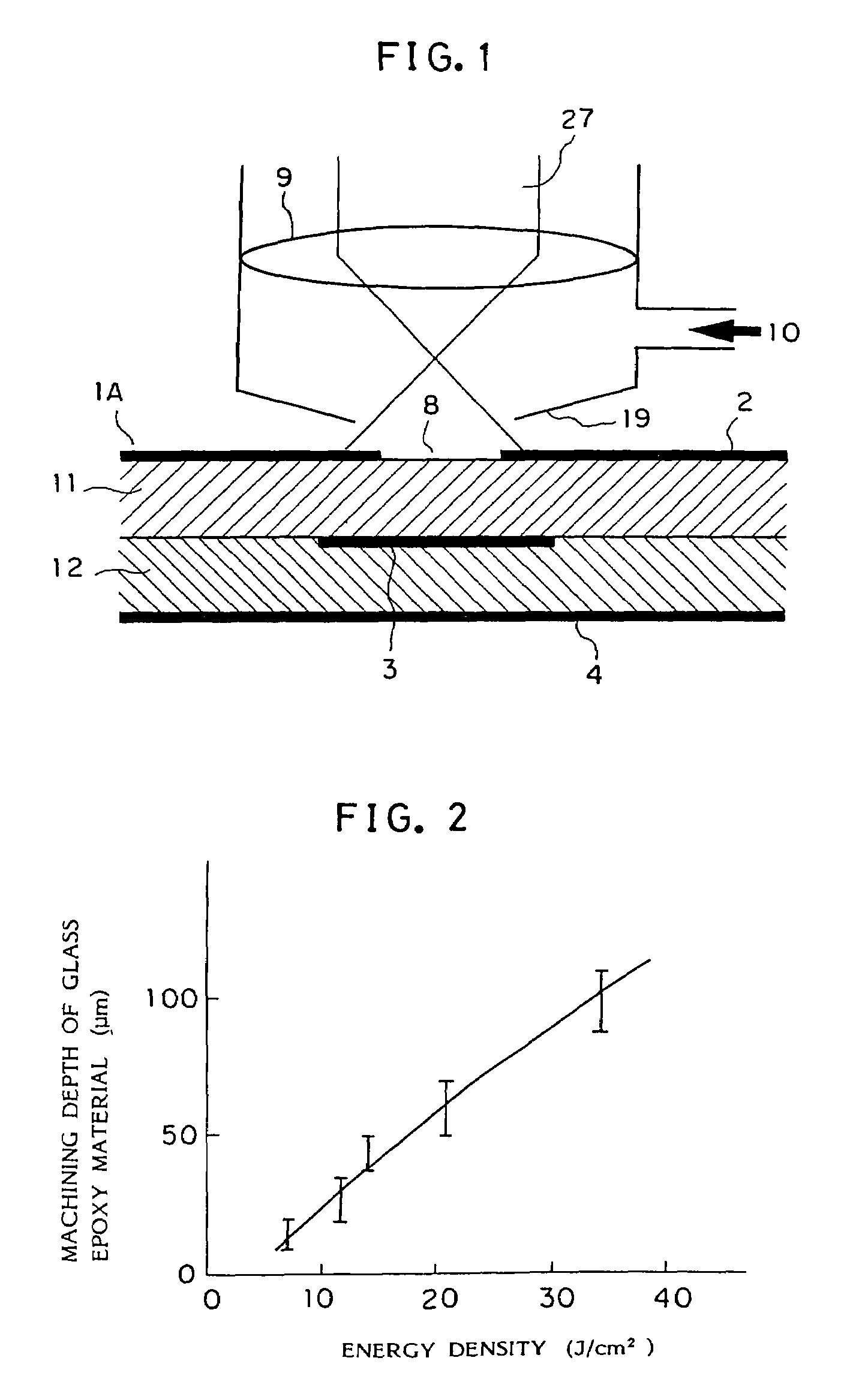
[0076]FIG. 1 is a typical diagram showing a laser beam machining method for a wiring board according to the embodiment 1 of the present invention. In the drawing, reference numeral 1A means a printed board (wiring board), 2, 3, and 4 are conductor layers (metallic layers) including copper foil, 8 is a copper foil removed portion formed in the top conductor layer 2 by etching, 9 is a ZnSe lens for convergence of a laser beam 27 radiated from a carbonic acid gas laser, and 10 is an assist gas for lens protection. Air is employed in the embodiment as the assist gas 10. Reference numerals 11 and 12 are insulating base materials, and 19 is a gas nozzle through which the assist gas 10 is ejected. Here, the copper foil removed portion 8 is formed in the conductor layer 2 at a portion corresponding to a machined portion of the insulating base material 11.

[0077]In the embodiment 1, a three-layer glass epoxy printed board (FR-4) with both sides coated with copper foil and a thickness of ...

embodiment 2

[0084

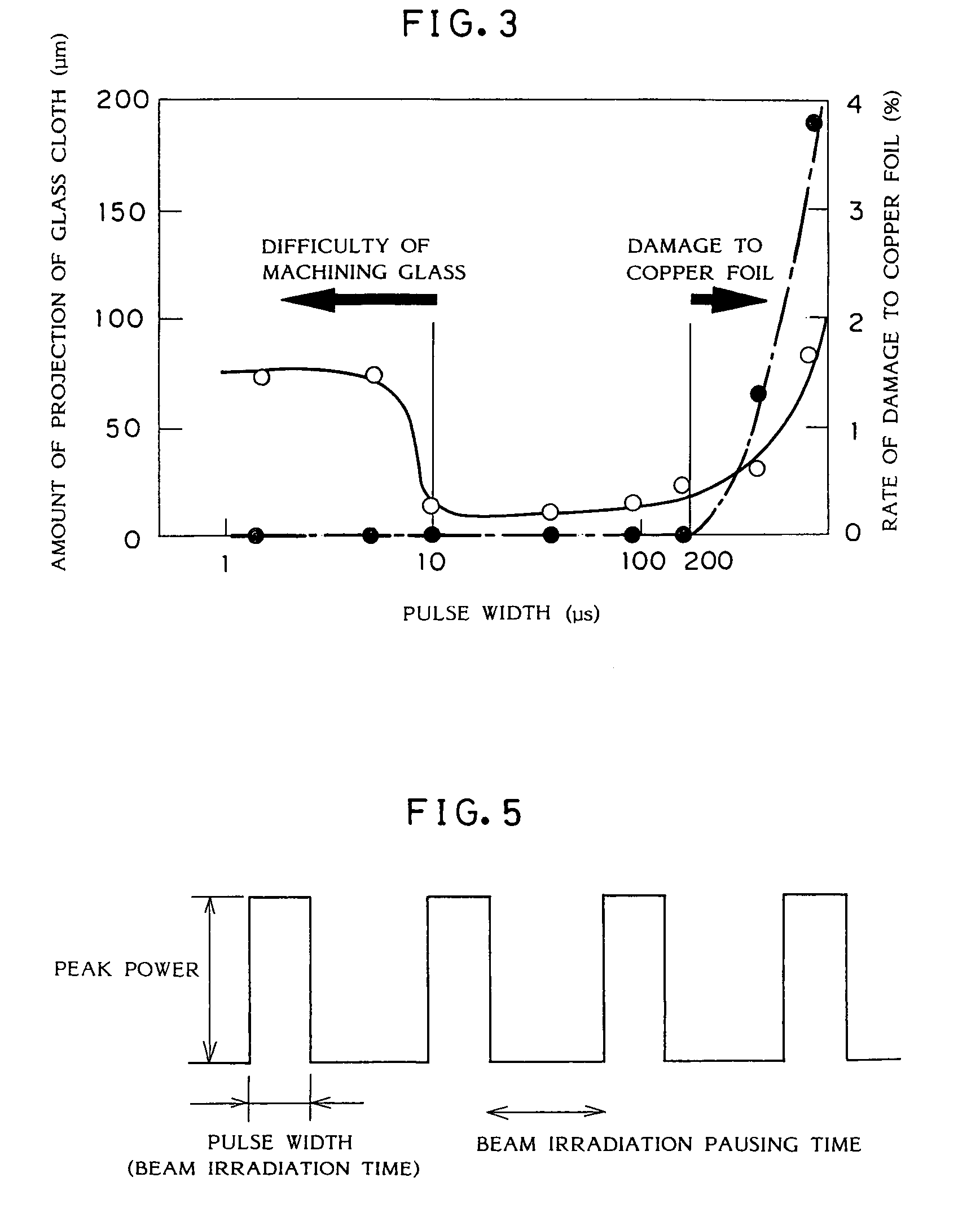
[0085]FIG. 4 is a typical diagram showing a laser beam machining method for a wiring board according to the embodiment 2 of the present invention. In the drawing, the same reference numerals are used for component parts identical with those in FIG. 1, and descriptions thereof are omitted. Further, in FIG. 4, reference numeral 1B means a multi-layer printed board, 5 is a conductor layer, 6 is a conductor layer on a rear surface of the multi-layer printed board 1B, 7 is metal deposited on an inner surface of a through-hole 17, and 13 and 14 are insulating base materials. FIG. 5 is a waveform diagram showing an irradiation pattern of a laser beam 27 in the embodiment 2.

[0086]In the embodiment 2, a five-layer glass polyimide board with a thickness of 400 μm was used as the printed board 1B. In a top conductor layer 2 and a bottom conductor layer 6, copper foil had a thickness of 18 μm, and etching was made to form copper foil removed portions 8 with a diameter of 200 μm in the cond...

embodiment 3

[0094

[0095]FIG. 8 is a waveform diagram showing an irradiation pattern of a laser beam in a laser beam machining method for a wiring board according to the embodiment 3 of the present invention. In the embodiment 3, as shown in FIG. 4 of the embodiment 2, a five-layer glass polyimide board with a thickness of 400 μm was used as a printed board 1B. In a top conductor layer 2 and a bottom conductor layer 6, copper foil had a thickness of 18 μm, and etching was made to form copper foil removed portions 8 with a diameter of 200 μm in the conductor layer 2 and the conductor layer 6 at positions corresponding to a conduction hole to be machined.

[0096]A description will now be given of the operation.

[0097]A laser beam 27 was emitted from a carbonic acid gas laser with a constant pulse width of 50 μs, and constant pulse energy of 280 mJ. Further, the laser beam 27 was condensed on the printed board 1B through a ZnSe lens 9 such that a laser beam diameter became 500 μm on a surface of the ma...


PUM

PropertyMeasurementUnit
timeaaaaaaaaaa
timeaaaaaaaaaa
thicknessaaaaaaaaaa

Abstract

In a laser beam machining method for a wiring board, a machined portion of the wiring board is irradiated with a pulsed laser beam for a beam irradiation time ranging from about 10 to about 200 μs and with energy density of about 20 J / cm2 or more, thereby machining the wiring board, for example, drilling for a through-hole and a blind via hole, grooving, and cutting for an outside shape.

Description

[0001]This is a divisional of Application No. 09 / 549,498 (Confirmation No. Not Yet Assigned) filed Apr. 14, 2000 now U.S. Pat. No. 6,373,026, which is a divisional of Application No. 08 / 690,140, filed Jul. 31, 1996, the disclosure of which is incorporated herein by reference.BACKGROUND OF THE INVENTION[0002]1. Field of the Invention[0003]The present invention relates to a machining method for a wiring board and a machining apparatus for a wiring board employing a laser beam for machining such as drilling for a through-hole, an inner via hole, and a blind via hole, grooving, and cutting for an outside shape of the wiring board referred to as so-called printed board, and more particularly to a machining method for a wiring board and a machining apparatus for a wiring board in which a fine conduction hole can rapidly and accurately be formed, and a carbonic acid gas laser oscillator to generate a pulsed laser beam most suitable for the above machining.[0004]2. Description of the Prior ...

Claims


Application Information

Patent Timeline
Patent Type & Authority Patents(United States)
IPC IPC(8): B23K26/38H05K3/00
CPCB23K26/385H05K3/0032H05K2203/0554H05K2203/081B23K26/389
Inventor KUROSAWA, MIKIFUKUSHIMA, TSUKASAMIZUNO, MASANORITAKENO, SHOZUIMORIYASU, MASAHARUKANEKO, MASAYUKI
Owner MITSUBISHI ELECTRIC CORP
Why Eureka
Try Eureka