Ion plasma beam generating device

a beam generation device and plasma technology, applied in the direction of discharge tube/lamp details, discharge tube/lamp details, electric discharge tubes, etc., can solve the problems of space charge emission not being possible, common non-uniform beams, and the possibility of atmospheric gasses and impurities in the chamber, etc., to achieve wide area, stable properties, and reduce electron emission

Active Publication Date: 2005-12-13
ADASTRA TECH
View PDF9 Cites 38 Cited by
  • Summary
  • Abstract
  • Description
  • Claims
  • Application Information

AI Technical Summary

Benefits of technology

[0012]The present objects are achieved with a low pressure chamber including at least one grid for plasma containment. A plasma is generated by a plasma source within the chamber. The plasma ions are accelerated through the grid to a high voltage cathode, a semiconductor slice. Impact of the ions on the cathode produces an electron beam having the cross-sectional dimension of the semiconductor slice. The high voltage cathode slice is preferably made of silicon that is doped in variable and graded amounts to produce a beam of desired characteristics, i.e. offsetting beam non-uniformities without doping. Alternatively, the cathode may be made of a semiconductor hybrid material, such as germanium or an alloy. Either of these options allows for a cathode in which the secondary electron emission is spatially designed to either decrease the electron emission in the center of the beam or increase the electron emission outwardly toward the peripheral edge of the beam. This selective doping of a semiconductor material provides for a wide area beam that is more uniform. The silicon cathode is very stable and is available in very precisely ...

Problems solved by technology

One technical challenge is to generate a uniform plasma that could provide an even areawise amount of energy to irradiate an object.
Beam non-uniformities are common.
In such devices, space charge emission is not possible and the electron density is dependent on the ion density and surface ...

Method used


Image

  • Ion plasma beam generating device
  • Ion plasma beam generating device
  • Ion plasma beam generating device

Examples


Embodiment Construction

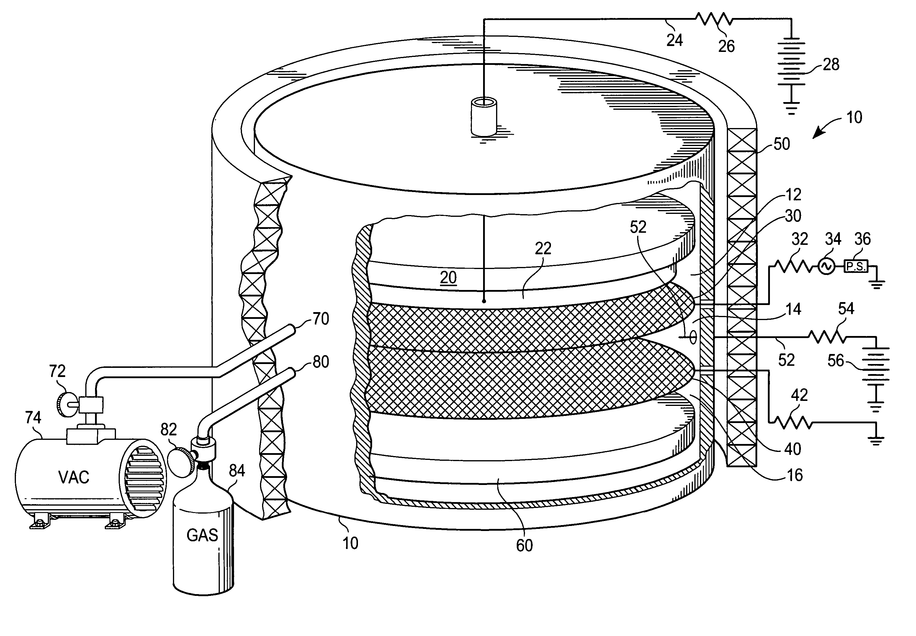
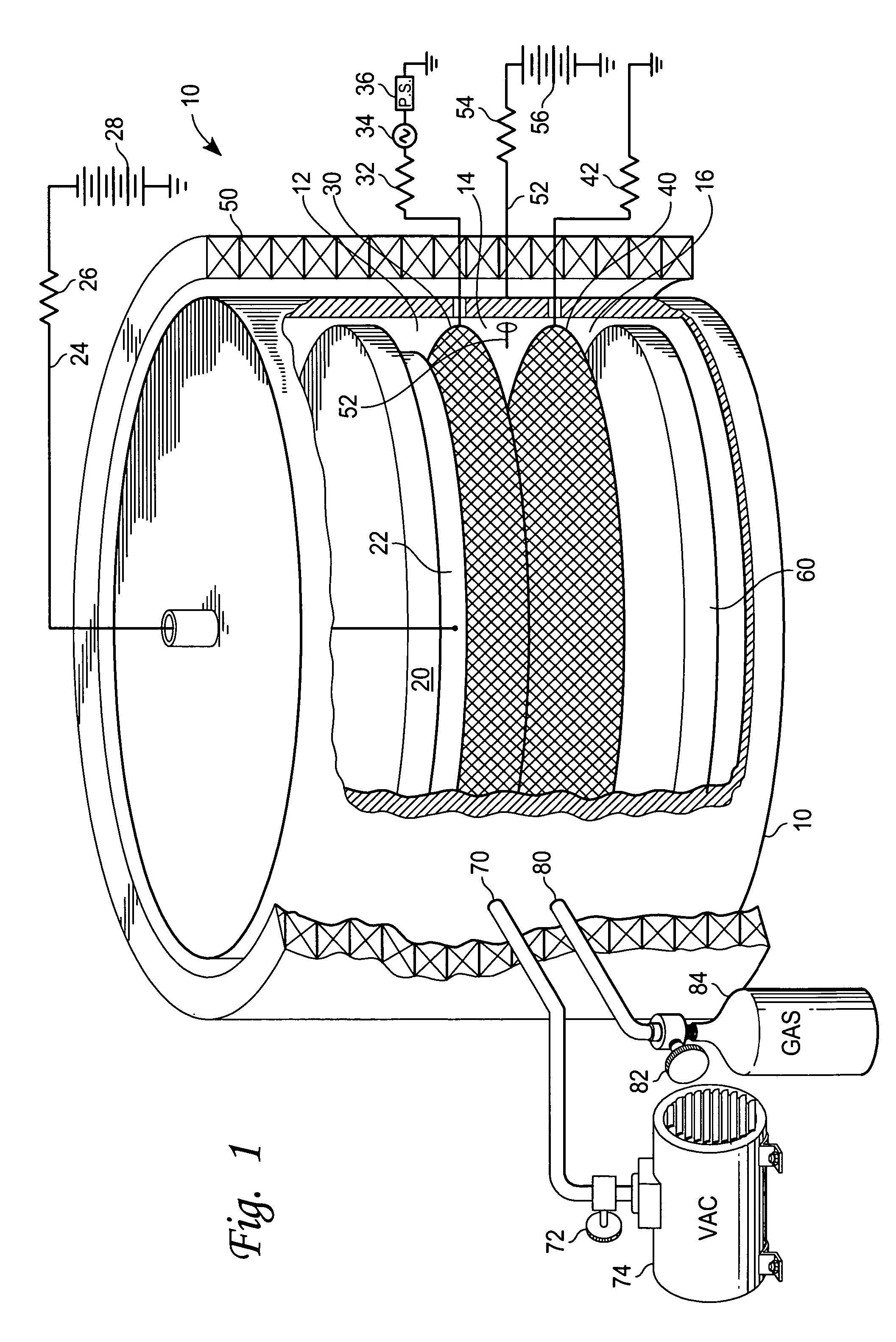
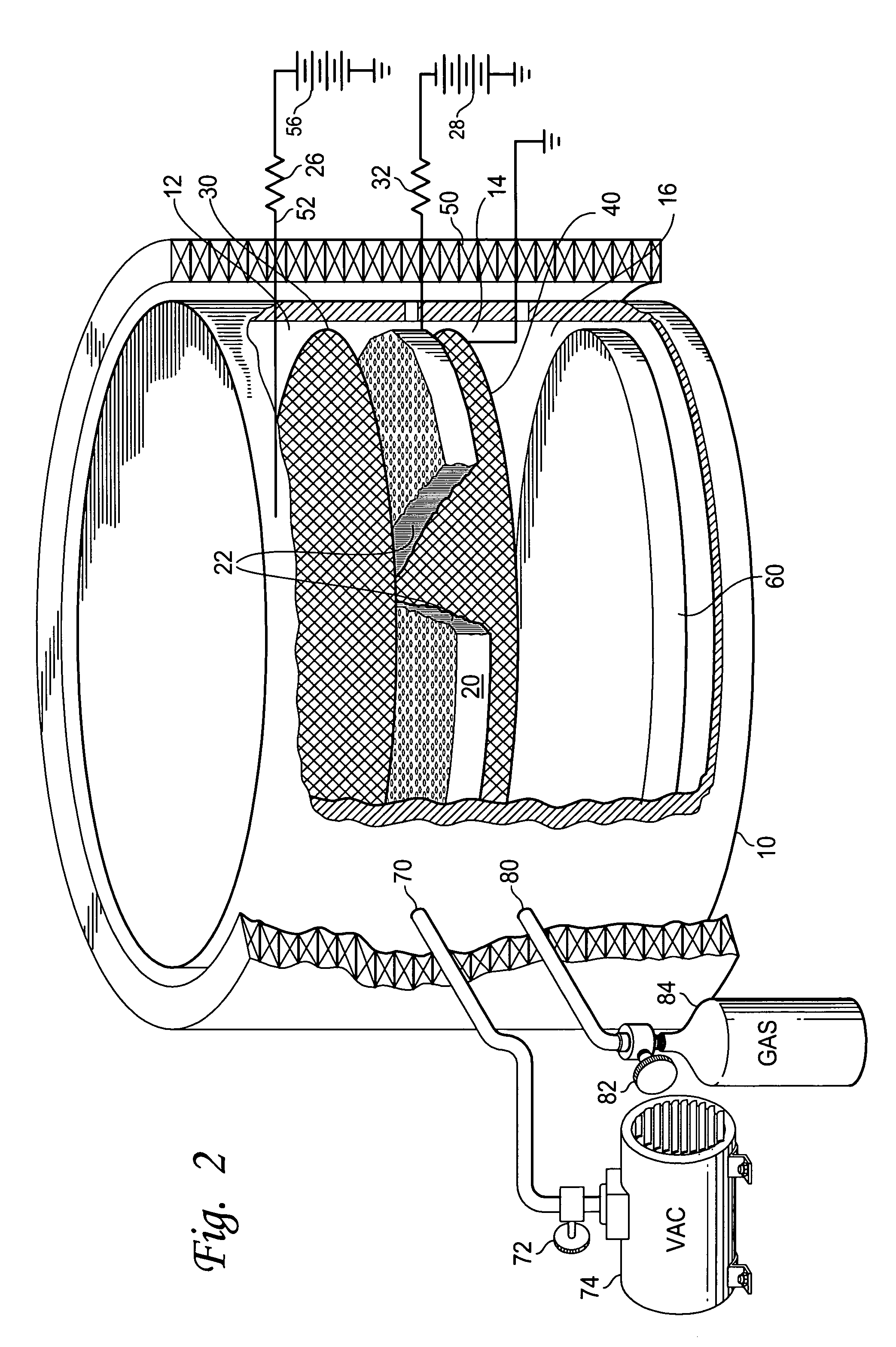
[0017]With respect to FIG. 1, plasma chamber 10 is a very low pressure vessel composed of three internal regions, an upper region 12, a middle region 14 and a lower region 16. The volume within plasma chamber 10 is gas tight, such that the atmosphere within the chamber may be controlled to near vacuum conditions. The areas through which components extend into the chamber (such as the attachment of the gas and vacuum lines, and wires extending into the chamber) may be sealed with O-ring gaskets to ensure the vacuum integrity within the chamber.

[0018]The walls of the chamber should be made of a non-magnetic material, such as a ceramic dielectric or stainless steel, so that a magnetic field can penetrate the chamber. The walls of the chamber may be made of aluminum and internally coated with a 2–3 mm. nickel coating.

[0019]The plasma will be initially generated in middle region 14. A low volume of gas flows in through inlet 80 from gas tank 84. Flow from tank 84 is controlled by valve 8...


PUM


Abstract

An electron beam device wherein a low temperature gaseous plasma is generated in a chamber divided by two parallel wire grids. A semiconductor wafer serves as a cathode drawing ions from the plasma to impinge on the wafer, generating secondary electrons that are accelerated toward an anode on the opposite side of the grids where a target resides. In order to have a beam with uniform cross-sectional flux characteristics, the semiconductor wafer is doped with a graded dopant concentration that promotes a uniform beam.

Description

CROSS-REFERENCE TO RELATED APPLICATION[0001]This application claims priority from U.S. provisional application No. 60 / 471,907 filed May 19, 2003.TECHNICAL FIELD[0002]The present invention relates to ion plasma devices for generating electron beams and, more specifically, to a wide area beam device.BACKGROUND OF THE INVENTION[0003]There is a present need for an irradiation device that can provide a uniform wide area beam. This would have a number of applications, including the processing of materials requiring electron beam exposure, such as in semiconductor manufacturing, sterilization, curing of polymers, etc. For example, in curing spin-on glass coatings on semiconductor wafers or CVD coatings, an electron beam may be used to drive off organic elements in the coating.[0004]One technical challenge is to generate a uniform plasma that could provide an even areawise amount of energy to irradiate an object. Uniform large area electron beams are usually generated by scanning a small be...

Claims


Application Information

Patent Timeline
IPC IPC(8): H01J3/02H01J7/24
CPCH01J3/021H01J3/025
Inventor WAKALOPULOS, GEORGE
Owner ADASTRA TECH
Why Eureka
Try Eureka