

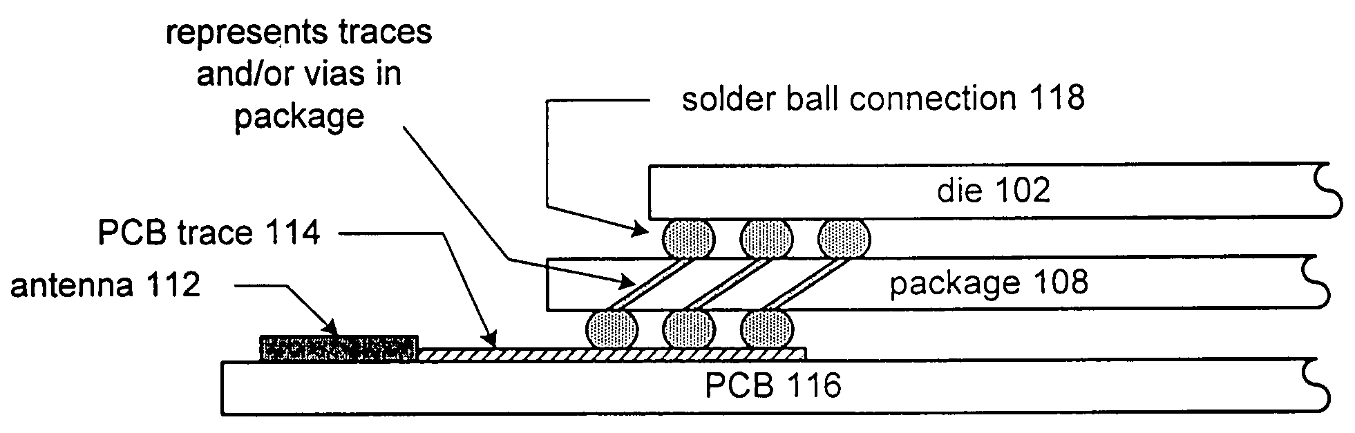
RFIC die-package configuration
a die-package and configuration technology, applied in the field of wireless communication devices, can solve the problems of limiting the overall performance of the radio transceiver, reducing the output power of the radio transmitter, and providing unacceptable levels of parasitic components in the conventional packaging, so as to reduce the adverse effects of parasitic components, improve the overall performance of the rfic, and reduce the level of parasitic components
- Summary
- Abstract
- Description
- Claims
- Application Information
AI Technical Summary
Benefits of technology
Problems solved by technology
Method used
Image

Examples
Embodiment Construction
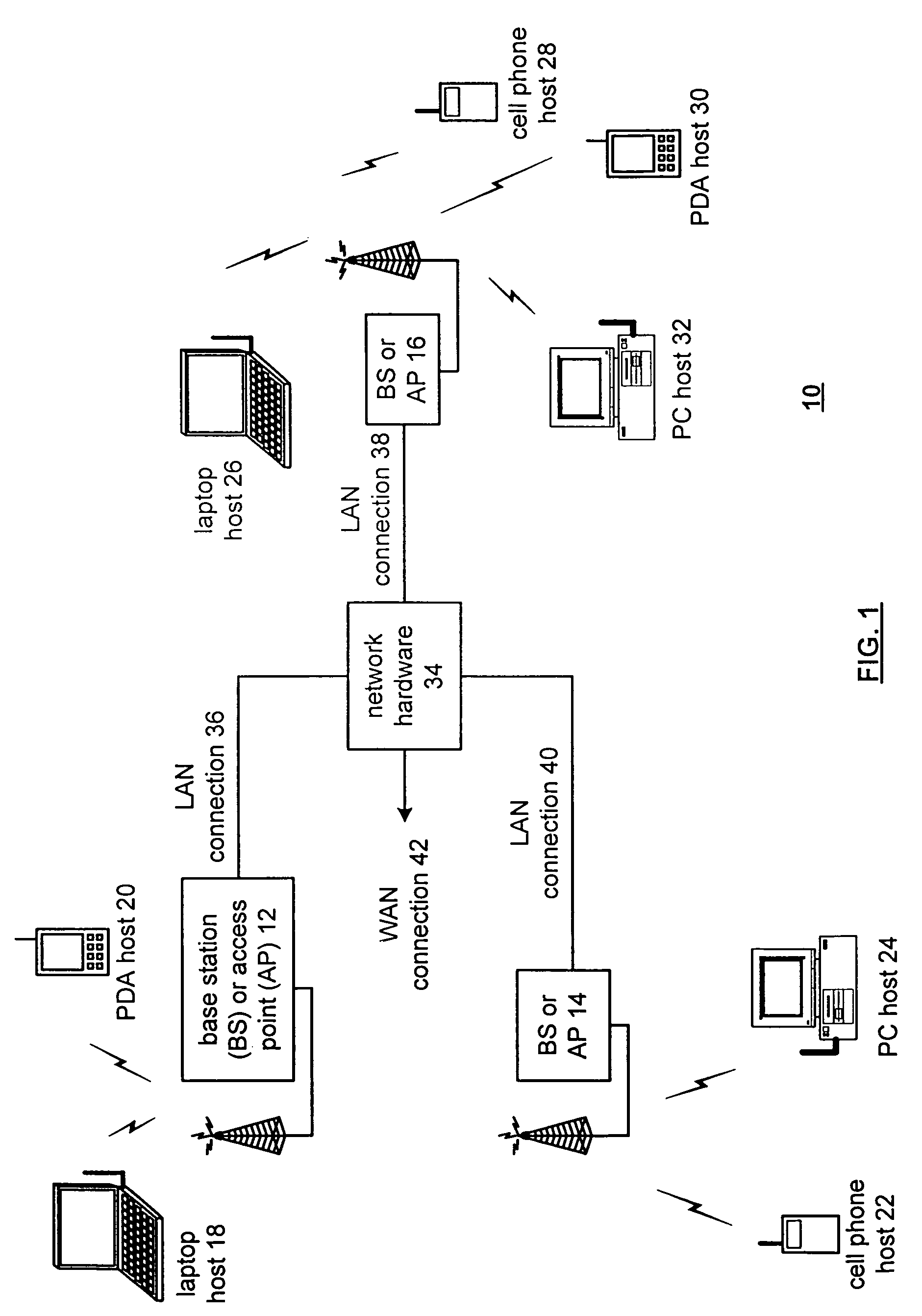
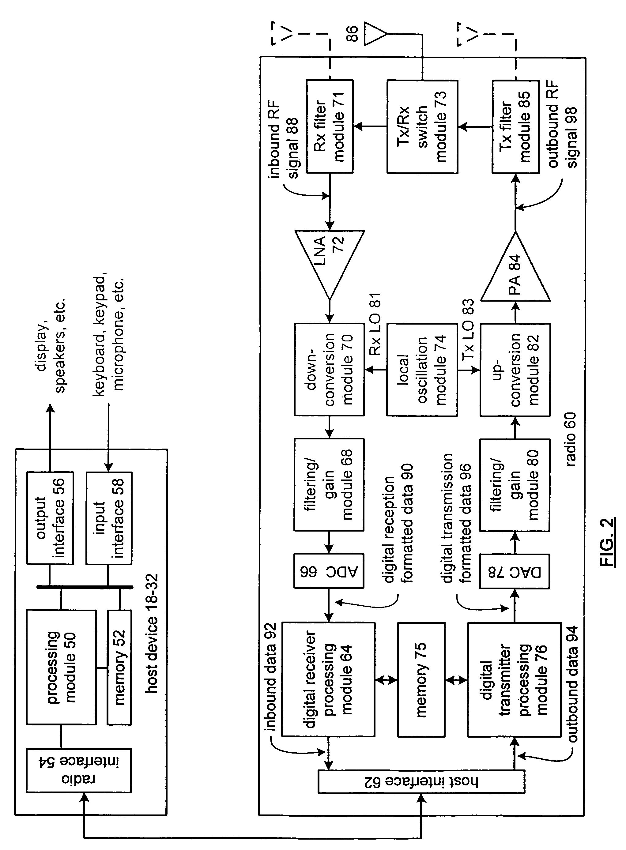
[0021]FIG. 1 is a schematic block diagram illustrating a communication system 10 that includes a plurality of base stations and / or access points 12–16, a plurality of wireless communication devices 18–32 and a network hardware component 34. The wireless communication devices 18–32 may be laptop host computers 18 and 26, personal digital assistant hosts 20 and 30, personal computer hosts 24 and 32 and / or cellular telephone hosts 22 and 28. The details of the wireless communication devices will be described in greater detail with reference to FIG. 2.
[0022]The base stations or access points 12–16 are operably coupled to the network hardware 34 via local area network connections 36, 38 and 40. The network hardware 34, which may be a router, switch, bridge, modem, system controller, et cetera provides a wide area network connection 42 for the communication system 10. Each of the base stations or access points 12–16 has an associated antenna or antenna array to communicate with the wirele...
PUM
| Property | Measurement | Unit |
|---|---|---|
| frequency | aaaaa | aaaaa |
| radio frequencies | aaaaa | aaaaa |
| radio frequencies | aaaaa | aaaaa |
Abstract
Description
Claims
Application Information