Method of making layered superlattice material with improved microstructure

a superlattice material and microstructure technology, applied in the direction of electrical equipment, semiconductor devices, capacitors, etc., can solve the problems of significant decrease in leakage current, increase in remnant polarization, and decrease in shorting problems, so as to improve surface morphology or smoothness, the effect of reducing shorting

Inactive Publication Date: 2006-02-21
SYMETRIX +1
View PDF7 Cites 4 Cited by
  • Summary
  • Abstract
  • Description
  • Claims
  • Application Information

AI Technical Summary

Benefits of technology

[0008]The invention overcomes the problems of porous surface morphology and crystal orientation in integrated circuit fabrication by modifying process steps in an integrated circuit process. In one aspect, the invention improves the surface morphology or smoothness by patterning the ferroelectric thin film prior to the final crystallization furnace anneal. Because the grain growth of the ferroelectric thin film mainly occurs during the final crystallization furnace anneal, patterning the ferroelectric thin film prior to this anneal decreases the shorting problems that occur during the patterning process with thin films having a large grain size. This eliminates the problems associated with patterning through thin films with large grain size. Preferably, the layered superlattice material is strontium bismuth tantalate, strontium bismuth tantalum niobate, or strontium bismuth niobate.
[0009]In another aspect, the invention further overcomes the problem of porous surface morphology and crystal orientation in the fabrication of layered superlattice material by incorporating a second rapid thermal anneal (RTA) after the patterning of preferably the top electrode, the ferroelectric thin film material and preferably the bottom electrode, but before the final crystallization furnace anneal. This second rapid thermal anneal successfully results in a significant decrease in the leakage current and an increase in the remnant polarization. It has been found that the second RTA after the patterning is particularly effective.
[0010]The invention further overcomes the problem of porous surface morphology and crystal orientation in integrated circuit fabrication by depositing a second layer of layered superlattice material over the first layered superlattice material thin film which is prepared by conventional methods. This second layer of layered superlattice material further reduces the surface roughness of first layered superlattice material thin films. It is preferably deposited by use of a sol-gel solution. In the preferred embodiment, first a single layer of layered superlattice material thin film is deposited by preferably KJC-MOD over the bottom electrode of a capacitor and then baked preferably in first and second bake steps. These steps are repeated until the designed thickness of the layered superlattice material thin film is achieved. Then an optional furnace anneal at 700° C. in oxygen is performed on the baked layered superlattice material thin film; then a second layer of layered superlattice material sol-gel solution is deposited on the substrate and baked, preferably in first and second bake steps, followed by a furnace anneal.
[0011]In a further aspect, the invention overcomes the problem of porous surface morphology and crystal orientation in integrated circuit fabrication by applying an exacting amount of ultraviolet (UV) radiation during the baking process. This UV photon energy created by the UV source during baking effectively decomposes the metalorganic compounds. Chemical bonds in metalorganic layered superlattice material solutions have various specified binding energies in accordance with each chemical bond. These binding energies are taken into consideration and the UV radiation source wavelength, UV radiation power density, and UV radiation exposure time are selected to fabricate a smoother layered superlattice material microstructure. Layered superlattice materials processed according to the invention showed no fatigue up to 1010 cycles of 3.0 volt bipolar stresses. By employing the modified UV radiation baking processes, the break down voltage (VBD) improved up to 12–13 volts and break down field (EBD) improved up to more than 1.1 MV / cm.

Problems solved by technology

Because the grain growth of the ferroelectric thin film mainly occurs during the final crystallization furnace anneal, patterning the ferroelectric thin film prior to this anneal decreases the shorting problems that occur during the patterning process with thin films having a large grain size.
This second rapid thermal anneal successfully results in a significant decrease in the leakage current and an increase in the remnant polarization.

Method used


Image

  • Method of making layered superlattice material with improved microstructure
  • Method of making layered superlattice material with improved microstructure
  • Method of making layered superlattice material with improved microstructure

Examples


example 1

Second Rapid Thermal Anneal After Patterning

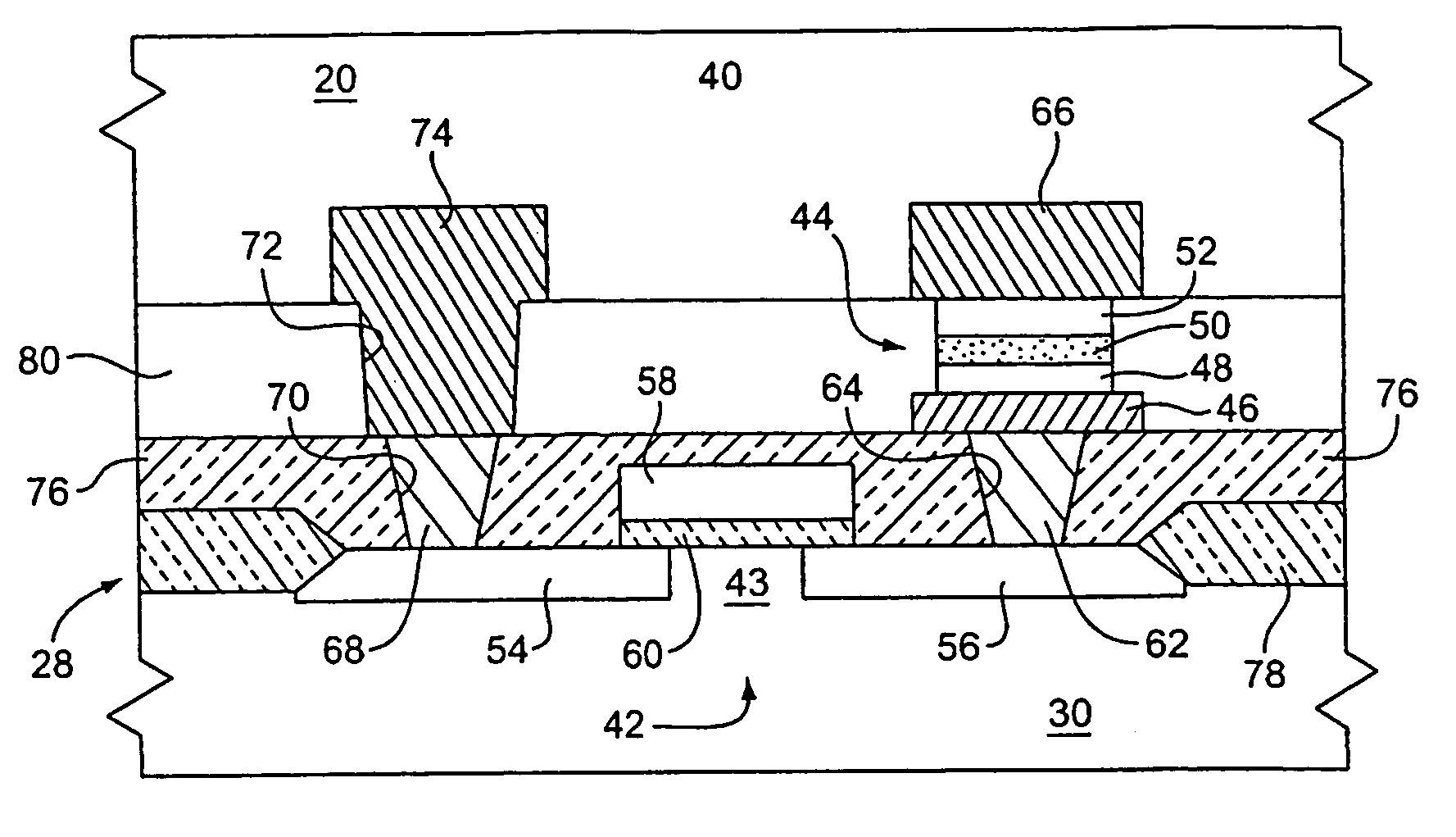
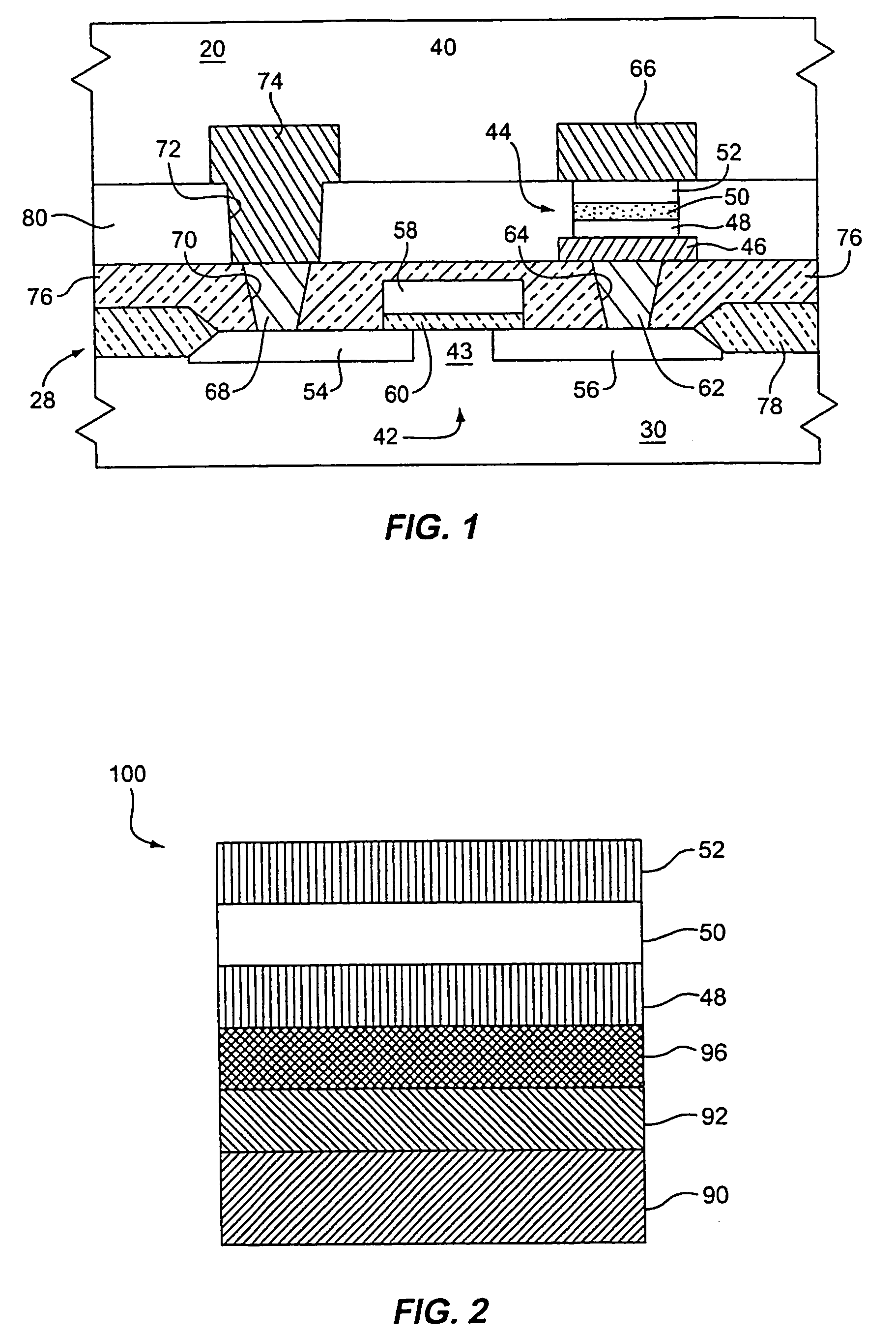
[0069]A substrate 28 including capacitor 44 was fabricated in which layered superlattice material layer 50 was layered superlattice material, more specifically, strontium bismuth tantalate (Sr0.9Bi2.2Ta2O9). The precursor solution molarity was approximately 0.10 moles per liter. A substrate 28 comprising a single crystal silicon layer 90, a 5000 Å thick layer 92 of silicon dioxide, a 200 Å thick layer 96 of titanium, and a 2000 Å thick layer 48 of platinum was prebaked at 800° C. in a diffusion furnace for 30 minutes with an oxygen flow of 6 liters / min. The precursor solution was deposited on the substrate 28 by KJC-MOD. Substrate 28 was spun at 2500 RPM for 30 seconds. Substrate 28 was then placed on a hot plate and baked in air at 160° C. for 1 minute. The precursor deposition and baking steps were repeated twice more. Substrate 28 was then placed on a hot plate and baked in air at 260° C. for 4 minutes. Substrate 28 was then transferred...

example 2

Formation of a Strontium Bismuth Tantalate Second Layer

[0072]A substrate 28 including capacitor 44 was fabricated in which layered superlattice material layer 50 was layered superlattice material, more specifically, strontium bismuth tantalate (Sr0.9Bi2.2Ta2O9). The precursor molarity was approximately 0.10 moles per liter. Substrate 28 comprising a single crystal silicon layer 90, a 5000 Å thick layer 92 of silicon dioxide, a 200 Å thick layer 96 of titanium, and a 2000 Å thick layer 48 of platinum was prebaked at 800° C. in a diffusion furnace for 30 minutes with an oxygen flow of 6 liters / min. The precursor solution was deposited on substrate 28 by KJC-MOD. Substrate 28 was spun at 2500 RPM for 30 seconds. Substrate 28 was then placed on a hot plate and baked in air at 160° C. for 1 minute. Substrate 28 was then baked in air at 260° C. for 4 minutes. Substrate 28 was then transferred to a rapid thermal anneal apparatus, then a rapid thermal annealing in oxygen of substrate 28 was...

example 3

Furnace Anneal After the Patterning Process

[0076]Substrate 28, including capacitor 44, was fabricated in which layered superlattice material layer 50 was layered superlattice material, more specifically, strontium bismuth tantalate (Sr0.9Bi2.2Ta2O9). The precursor molarity was approximately 0.10 moles per liter. Substrate 28 comprising a single crystal silicon layer 90, a 5000 Å thick layer 92 of silicon dioxide, a 200 Å thick layer 96 of titanium, and a 2000 Å thick layer 48 of platinum was prebaked at 800° C. in a diffusion furnace for 30 minutes with an oxygen flow of 6 liters / min. The precursor solution was deposited on the substrate by KJC-MOD. Substrate 28 was spun at 2500 RPM for 30 seconds. Substrate 28 was then placed on a hot plate and baked in air at 160° C. for 1 minute. Substrate 28 was then baked in air at 260° C. for 4 minutes, then the steps of applying the precursor through the second baking step were repeated once more. Substrate 28 was then transferred to a rapid ...


PUM

PropertyMeasurementUnit
temperatureaaaaaaaaaa

Abstract

In the manufacture of an integrated circuit, a first electrode (48) is formed on a substrate (28). In a first embodiment, a strontium bismuth tantalate layer (50) and a second electrode (52) are formed on top of the first electrode (48). Prior to the final crystallization anneal, the first electrode (48), the strontium bismuth tantalate layer (50) and the second electrode (52) are patterned. The final crystallization anneal is then performed on the substrate (28). In a second embodiment, a second layer (132) of strontium bismuth tantalate is deposited on top of the strontium bismuth tantalate layer (50) prior to the forming of the second electrode (52) on top of the first and second layers (50), (132). In a third embodiment, a carefully controlled UV baking process is performed on the strontium bismuth tantalate layer (50). In a fourth embodiment, an additional rapid thermal annealing process is performed on a substrate subsequent to the patterning process and prior to the final crystallization annealing process.

Description

[0001]This application is a national stage entry of PCT / US01 / 45392, with international filing date Oct. 30, 2001 which claims priority from provisional application 60 / 244,809 filed Oct. 31, 2000 which claims priority from provisional application 60 / 274,465 filed Mar. 9, 2001 which claims priority from provisional application 60 / 285,123 filed Apr. 20, 2001.BACKGROUND OF INVENTION[0002]1. Field of the Invention[0003]This invention pertains to the fabrication of integrated circuits utilizing thin film layered superlattice material, and more particularly to processes for improving the microstructure of such thin films.[0004]2. Statement of the Problem[0005]Layered superlattice material thin films have been a very strong candidate for high density ferroelectric random access memories (FeRAMs). However, some problems in the layered superlattice material thin film have been pointed out, such as low remnant polarization (Pr), high crystallization temperature and surface roughness in compari...

Claims


Application Information

Patent Timeline
Patent Type & Authority Patents(United States)
IPC IPC(8): H01L21/00H01L21/02H01L21/311H01L21/314H01L21/316H01L21/8246H01L27/115
CPCH01L21/02197H01L21/02282H01L28/55H01L27/11502H01L27/11507H01L21/31122H01L21/31691H10B53/30H10B53/00
Inventor KARASAWA, JUNICHIJOSHI, VIKRAM
Owner SYMETRIX
Why Eureka
Try Eureka