Thermoelectric conversion material and method of producing the same

a technology of thermoelectric conversion material and thermoelectric conversion method, which is applied in the direction of thermoelectric device junction material, thermoelectric device manufacture/treatment, electrical apparatus, etc., can solve the problems of high seebeck coefficient, difficult to produce a uniform composition with melting or zl, and low thermal conductivity, and achieve the effect of reducing thermal conductivity

Inactive Publication Date: 2006-02-21
SUMITOMO SPECIAL METAL CO LTD
View PDF2 Cites 55 Cited by
  • Summary
  • Abstract
  • Description
  • Claims
  • Application Information

AI Technical Summary

Benefits of technology

[0008]The inventors discovered that doping pure silicon with various elements, such as doping silicon with both a trace amount of a Group III element or Group V element and a small amount of a Group IV element, makes it possible to lower thermal conductivity, and the Seebeck coefficient will be equivale

Problems solved by technology

Also, silicon and germanium have a state in which there is a broad liquidus and solidus for complete solid solution, and it is difficult to produce a uniform composition with melting or ZL (zone leveling), to name just two of the problems which have impeded industrial application.
For these reasons, the above-mentioned materials have not fou

Method used


Image

  • Thermoelectric conversion material and method of producing the same
  • Thermoelectric conversion material and method of producing the same
  • Thermoelectric conversion material and method of producing the same

Examples


example 1

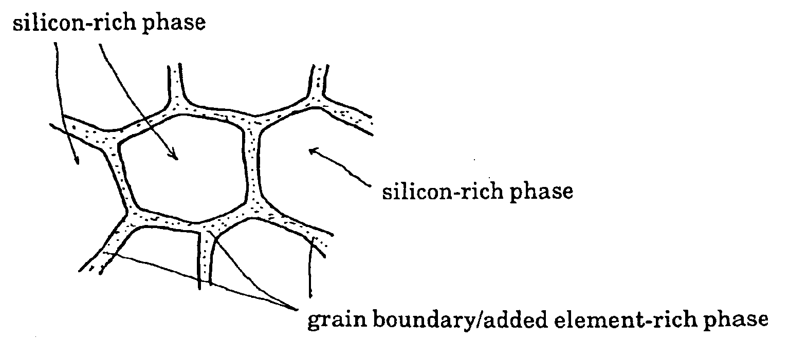
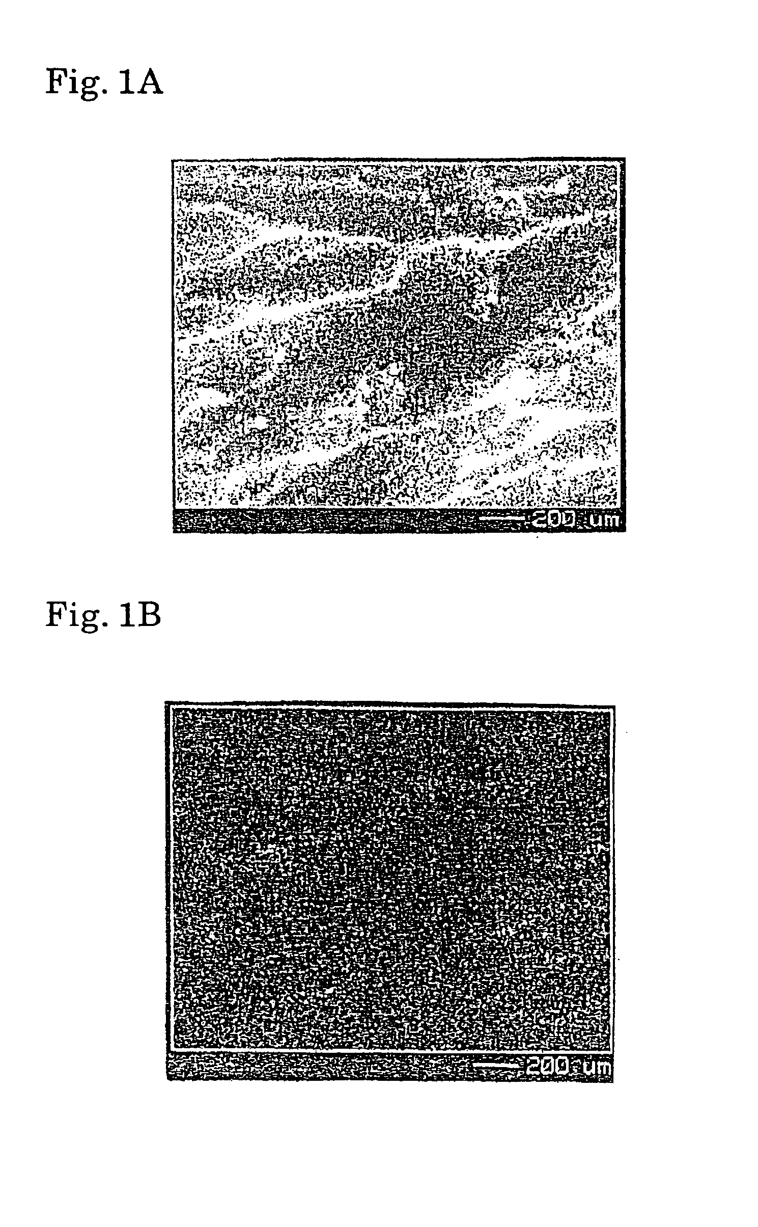
[0098]High-purity silicon (10N) and a added element (dopants that generate carriers are labeled Ap and An, while added elements that do not generate carriers are labeled Bnc; the same applies to all the added elements in the following examples) were compounded as shown in Table 1 and then arc-melted in an argon gas atmosphere to produce p- and n-type silicon thermoelectric conversion semiconductors. The temperature in the arc melting was approximately 1900K, and the molten material was cooled at a rate of 50 to 100 K / sec by a water-cooled copper base. The average crystal grain size of the obtained material was approximately 50 to 100 μm.

[0099]The button-shaped ingots thus obtained were cut to sizes of 5×5×15 mm, 10×10×2 mm, and 10 (outside diameter)×2 mm, and the Seebeck coefficient, Hall coefficient (including carrier concentration and electrical conductivity), and thermal conductivity were measured for each. The measurement values at 1100K and the Figure of merit (ZT=S2T / ρκ) are s...

example 2

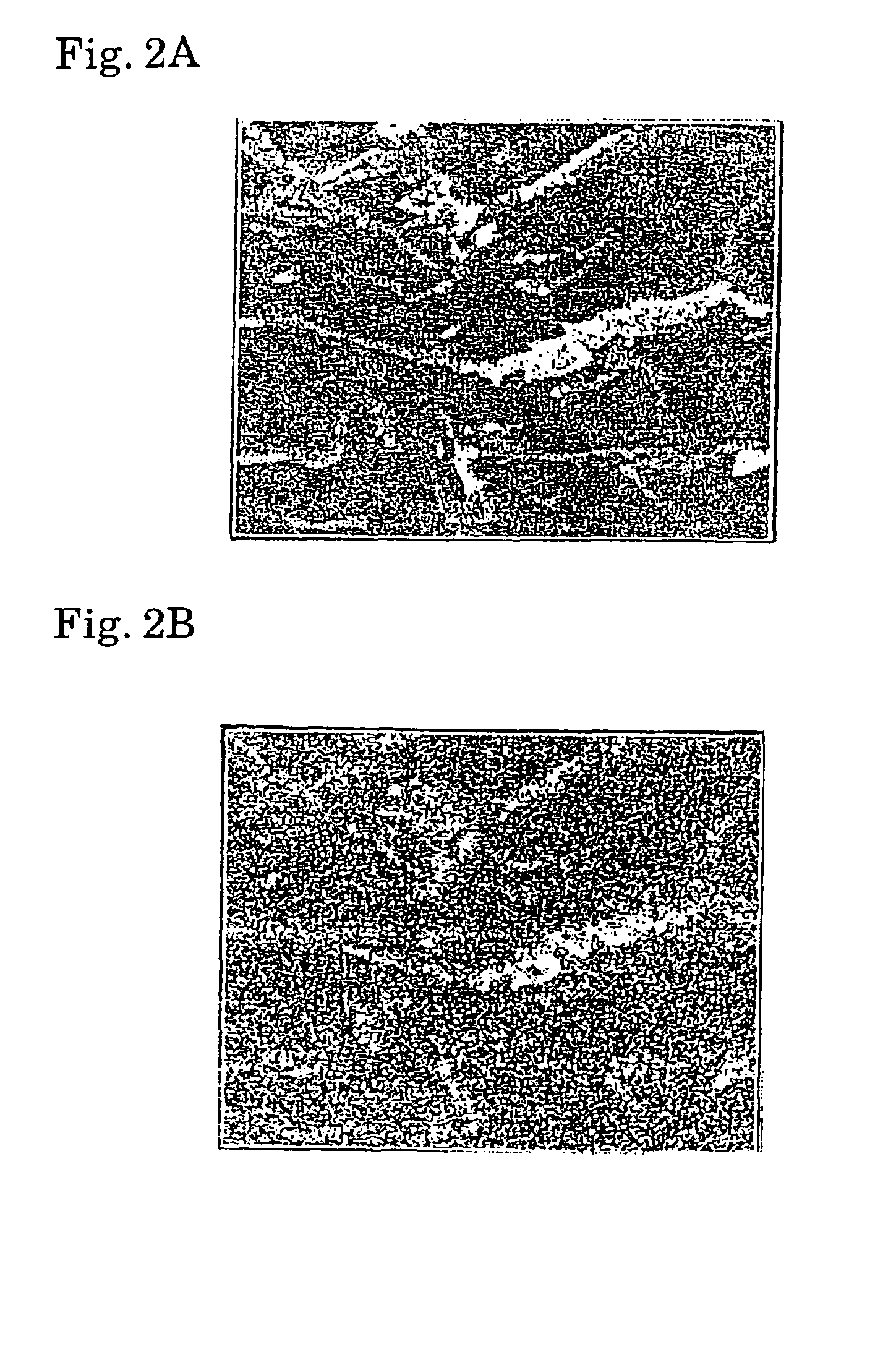
[0101]In order to produce p- and n-type silicon thermoelectric semiconductors, high-purity silicon (10N) and added elements were compounded as shown in Table 3, after which this product was put in a graphite crucible and melted in a high-frequency melting furnace in a vacuum (10−4 Torr). The melting temperature was approximately 1900K, the casting temperature was approximately 1800K, and the melt was cast into a mold with a thickness of 10 mm. The cooling rate of the molten material was 10 to 50 K / sec, and the average crystal grain size of the material was approximately 100 to 500 μm.

[0102]The ingots thus obtained were cut to sizes of 5×5×15 mm, 10×10×2 mm, and 10 (outside diameter)×2 mm, and the Seebeck coefficient, Hall coefficient (including carrier concentration and electrical conductivity), and thermal conductivity of each were measured by the same methods as in Example 1. Table 4 shows the measured values at 1100K and the Figure of merit (ZT=S2T / ρκ).

example 3

[0103]In order to produce p- and n-type silicon thermoelectric semiconductors, high-purity silicon (10N) and added elements were compounded as shown in Table 5, after which this product was put in a graphite crucible and melted in a high-frequency melting furnace in a vacuum (10−4 Torr), and it was confirmed that the components melted uniformly at approximately 1800K.

[0104]After this, the upper part of the above-mentioned graphite crucible was lowered to 1700K, silicon seed crystals were brought into contact with the top of the melt, and the melt was slowly pulled up. The inside diameter of the crucible was 100 mm, the pulling rate was 0.3 to 1 mm / sec, and the pulled crystals were vibrated once every five seconds in order to render them polycrystalline. The average crystal grain size of the obtained material was approximately 1 to 10 μm.

[0105]The ingots thus obtained were cut to sizes of 5×5×15 mm, 10×10×2 mm, and 10 (outside diameter)×2 mm, and the Seebeck coefficient, Hall coeffic...


PUM


Abstract

A thermoelectric conversion material is formed of a polycrystal structure of crystal grains composed of a silicon-rich phase, and an added element-rich phase in which at least one type of added element is deposited at the grain boundary thereof, the result of which is an extremely large Seebeck coefficient and low thermal conductivity, allowing the thermoelectric conversion rate to be raised dramatically, and affording a silicon-based thermoelectric conversion material composed chiefly of silicon, which is an abundant resource, and which causes extremely low environmental pollution.

Description

TECHNICAL FIELD[0001]This invention relates to a novel thermoelectric conversion material in which pure silicon is made to contain various types of added element, and more particularly relates to a silicon-based thermoelectric conversion material having a polycrystal structure, characterized in that the crystal structure comprises crystal grains composed of a silicon-rich phase, and a added element-rich phase in which at least one type of added element is deposited at the grain boundary thereof, the result of which is an extremely large Seebeck coefficient and low thermal conductivity of 50 W / m·K or less, allowing the thermoelectric conversion rate to be raised dramatically, and affording a silicon-based thermoelectric conversion material composed chiefly of silicon, which is an abundant resource, and which causes extremely little environmental pollution.BACKGROUND ART[0002]Thermoelectric conversion elements are devices that are expected to see practical use because of their efficie...

Claims


Application Information

Patent Timeline
IPC IPC(8): H01L35/20H01L35/12H01L35/16H01L35/22H01L35/34
CPCH01L35/34H01L35/22H10N10/855H10N10/01H10N10/851
Inventor SADATOMI, NOBUHIROYAMASHITA, OSAMUSAIGO, TSUNEKAZUNOUMI, MASAO
Owner SUMITOMO SPECIAL METAL CO LTD
Why Eureka
Try Eureka