Anti tamper encapsulation for an integrated circuit

Inactive Publication Date: 2006-02-28
UNIVERSAL IMAGING IND LLC
View PDF18 Cites 257 Cited by
  • Summary
  • Abstract
  • Description
  • Claims
  • Application Information

AI Technical Summary

Benefits of technology

[0010]The present invention seeks to provide an improved apparatus and method for protecting the content

Problems solved by technology

However, research has shown that any chip case can be attacked by some method (for example, acids, bases, solvents, plasma or reactive ion etch, focussed ion beam, laser or mechanical milling), and that the modification of the encapsulation to resist one of these methods tend to make it weaker against others.
However, whilst such approaches may protect a chip in the active state, they cannot protect a chip which is without power

Method used


Image

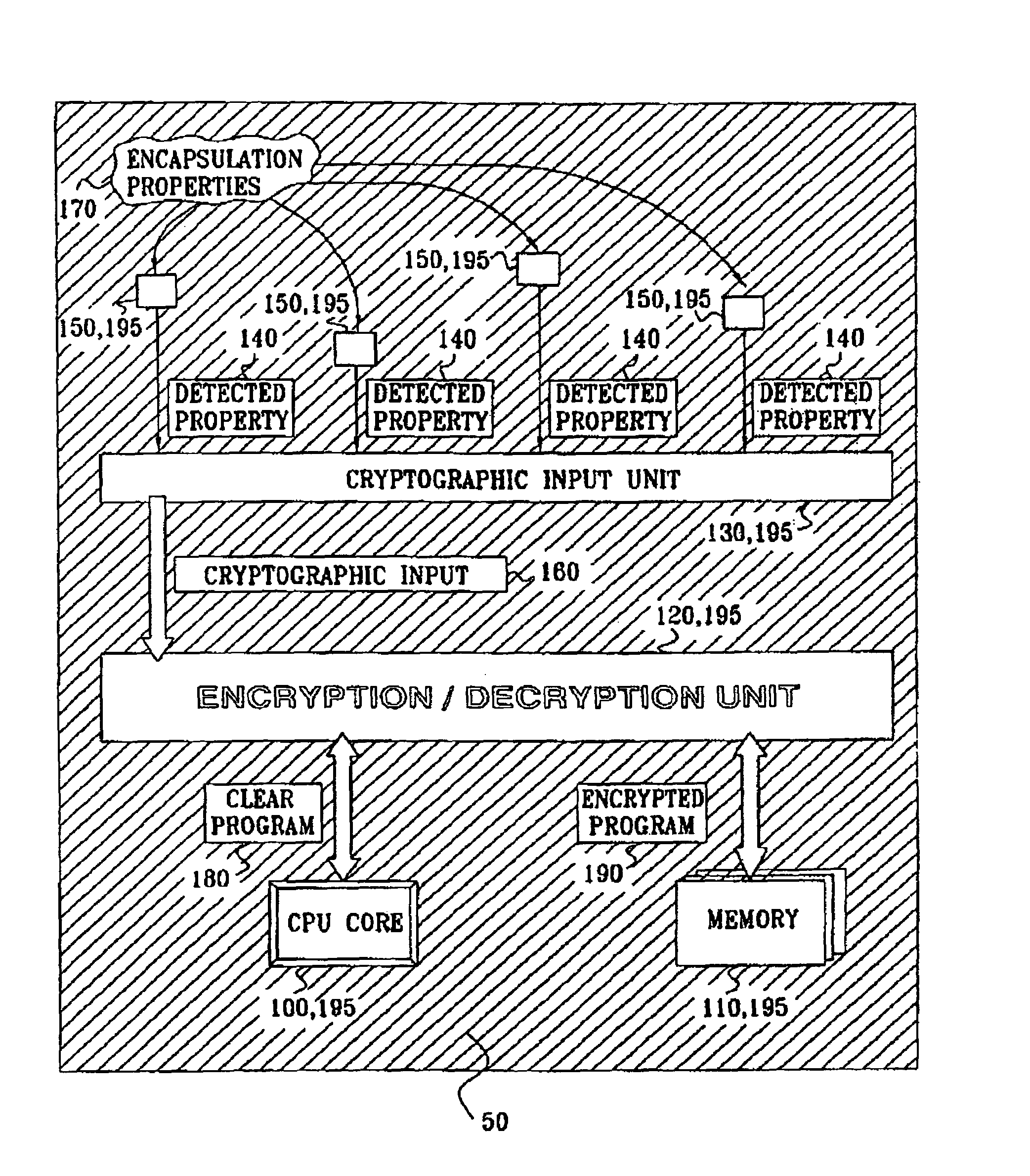
  • Anti tamper encapsulation for an integrated circuit
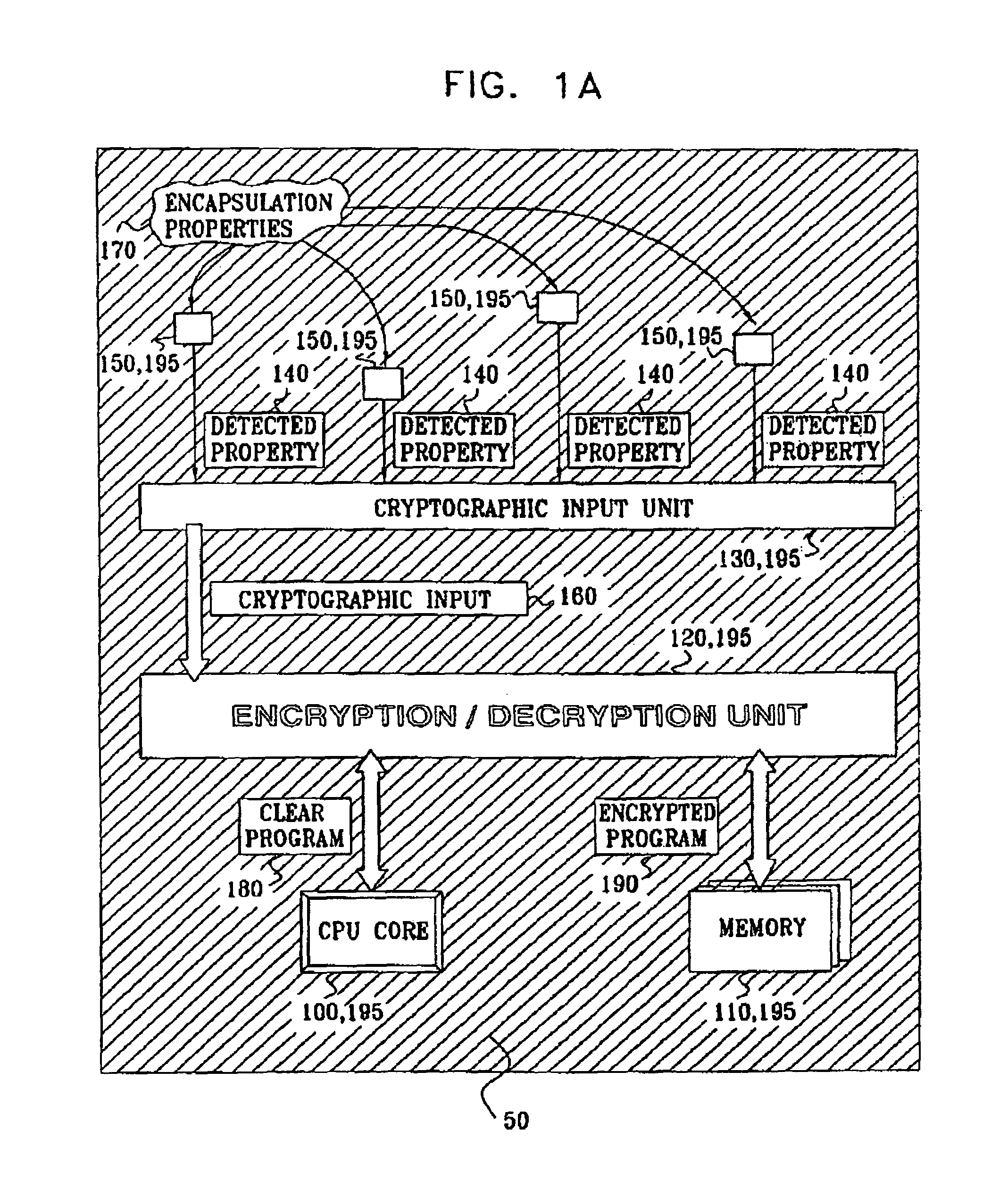
  • Anti tamper encapsulation for an integrated circuit
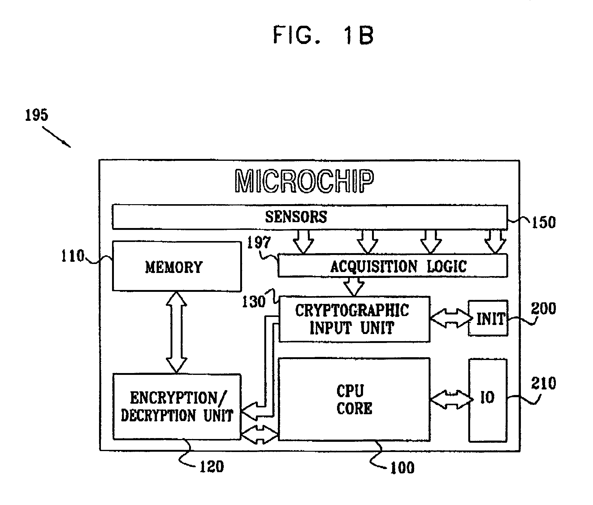
  • Anti tamper encapsulation for an integrated circuit

Examples


second embodiment

[0110]Referring to FIGS. 5a, and 5b, in this embodiment, the sensors 150 are magnetic field sensors such as Hall effect sensors, which may comprise a thin film of Indium Arsenide in an opening in the upper layer of the chip. The encapsulation 50 surrounds the device substrate 350 on both sides, and comprises an epoxy resin matrix 363. Within the matrix, a plurality of particles 360 are provided, of various sizes, shapes and / or magnetic permeabilities. These particles may be made out of Ni—Co—Fe alloy (i.e. a Ferrite alloy).

[0111]A pair of plate-shaped permanent magnets 365a, 365b are provided above and below the encapsulation layers 50, and bonded thereto by the epoxy resin 363. The magnets 365a, 365b are arranged with their poles aligned in the same direction, which in this embodiment is conveniently perpendicular to the plates 365.

[0112]Surrounding the plates 365 and encapsulation 50 is an outer casing 370 of soft magnetic core material. The effect of the casing 370 is to confine ...

third embodiment

tance Sensing

[0116]FIG. 6 shows structure of an embodiment in which local variations in the resistivity of the encapsulation are used to generate the key.

[0117]In this case, the sensors 150 comprise conductive openings in contact with the encapsulation 50, and are individually connectable to a voltage supply line and to a ground line. In use, one of the sensors 381 is connected to a voltage supply line and another 383 to the earth line. The current passing through either of the sensors (provided through a current sensing resistor) provides the sensor output.

[0118]In this embodiment, the encapsulation 50 surrounds the semiconductor substrate 350 of the device.

[0119]Within the epoxy resin matrix 363, a conductive powder having a relatively high electrical resistance such as graphite is intermixed. Alternatively, semiconductive materials such as Gallium, Copper Oxide or Selenium may be used.

[0120]Additionally, conductive particles such as strands of copper wire of varying lengths, widt...

fourth embodiment

ce Sensing

[0124]This embodiment has substantially the same structure as the last embodiment, except where differences are mentioned.

[0125]In this embodiment, within the casing 390 (which may be omitted if desired in this embodiment) an inner conductive layer 391 of, for example, aluminium is provided, in electrical contact with the encapsulation 50, and connected to the earth pin of the integrated circuit.

[0126]In this embodiment, each of the sensors 150 is selectively connectable to a supply line, via a current sensing resistor. To read the resistance of the encapsulation path directly above each of the sensors 392, 394, 396, 398, each one in turn is connected to the supply line, and the current through each flowing through the sensor and the encapsulation to the grounded metal layer 391 is measured through the current sensing resistor. In this way, resistances R1–R5 from the sensors 392, 394, 396, 398, 400 are successively measured in a scan. Again, differential measurements are p...


PUM


Abstract

An integrated circuit device comprising: a circuit which uses encryption; and an encapsulation packaging layer; in which the circuit is responsive to at least one physical parameter of the encapsulation to apply the encryption and/or decryption by reading the key therefrom, so that tampering with the encapsulation to gain access to the circuit causes the encryption and/or decryption to fail.

Description

CROSS-REFERENCE TO RELATED APPLICATIONS[0001]This application is related to the following U.S. Provisional Patent Application, by the present inventors, incorporated by reference herein, with priority claimed for all commonly disclosed subject matter: “Microchip Encapsulation with Encryption Key”, U.S. Ser. No. 60 / 173,994 filed 30 Dec. 1999.FIELD OF THE INVENTION[0002]The present invention relates to apparatus and methods for the protection of security sensitive content (e.g. data, program or cryptographic information) stored in memory within an integrated circuit assembly (such as an electrical integrated circuit or computer chip), from tampering. Examples of such integrated circuits are smart cards, microcontrollers, microprocessors or ASICs, as used for example in electronic banking, cash machines, subscription TV, mobile phones or the like.BACKGROUND OF THE INVENTION[0003]Various methods of preventing tampering with integrated circuits are known. One approach is to concentrate o...

Claims


Application Information

Patent Timeline
IPC IPC(8): H01L23/02G06F12/14G06F21/10G06F21/60G06F21/62G06F21/64G06F21/75G06F21/86G06F21/87G06K19/073H01L21/822H01L23/58H01L27/04H04L9/08H04L9/10
CPCG06F21/86H01L23/573G06K19/073G06K19/07372H01L23/576G09C1/00G06F21/87H04L9/0866H01L23/57H04L9/002H04L9/06H04L2209/12Y10S257/922H01L2924/0002H01L2924/00H01L2924/181H01L2924/00012H01L23/58
Inventor KOMMERLING, OLIVERKOMMERLING, FRITZ
Owner UNIVERSAL IMAGING IND LLC
Why Eureka
Try Eureka