Semiconductor device

a technology of semiconductors and devices, applied in the direction of transistors, digital storage, instruments, etc., can solve the problems of optimum circuits and layouts of cams, and achieve the effect of reducing the number of contact holes and reducing the noise of data lines

Inactive Publication Date: 2006-03-07
HITACHI LTD
View PDF9 Cites 123 Cited by
  • Summary
  • Abstract
  • Description
  • Claims
  • Application Information

AI Technical Summary

Benefits of technology

[0006]In order to reduce the manufacturing cost of the CAM, it is necessary to improve the yield of the CAM. Moreover, it is possible to enhance the performance of an LSI by mounting a large number of CAMs on the same chip. For this purpose, however, it is necessary to reduce the area of a memory cell in the CAM. In order to improve the consumed power or operating speed of the CAM, it is effective to form the CAM to be small, thereby reducing a wiring length in the CAM as greatly as possible. In order to enhance the reliability of data read from the CAM, it is necessary to reduce the noise of a reading data line.
[0009]It is another object of the invention to provide a technique for reducing the noise of a match line in a CAM.
[0010]It is a further object of the invention to provide a technique for reducing the noise of a data reading data line in a CAM.
[0014]According to the means, the data line is shared by the first storage portion and the second storage portion, and furthermore, the first transistor coupled to the first comparison data line is connected to the second transistor coupled to the storage node of the first storage portion in series to form the first comparing circuit, and the third transistor coupled to the second comparison data line is connected to the fourth transistor coupled to the storage node of the second storage portion in series to form the second comparing circuit. Consequently, it is possible to enhance a symmetry in the layout of a diffusion layer and a wiring layer and to achieve the easiness of a layout in which a memory cell is line symmetrical with respect to a center line passing through a center thereof. The memory cell is caused to have such a layout that it is line symmetrical with respect to a center line passing through a center thereof. Consequently, a manufacturing process condition can easily be optimized. Thus, a variation in a manufacturing process can be reduced and the microfabrication of a memory cell can be carried out, and furthermore, a semiconductor chip area can be decreased and the number of acquired chips and a yield can be improved so that a reduction in a manufacturing cost can be achieved.
[0018]By connecting the first comparing circuit and the second comparing circuit to the match line in common through a common contact hole, it is possible to achieve a reduction in the number of contacts.
[0022]The data line and the comparing data line are formed by the same wiring layer and a power wiring is provided between the data line and the comparing data line. By causing the power wiring to exhibit a shielding function, it is possible to achieve a reduction in a noise in the data line.

Problems solved by technology

However, the patent document 1 has described the layout of an SRAM cell formed by six MOS transistors and has not described an optimum circuit for the CAM and a layout thereof.

Method used


Image

  • Semiconductor device
  • Semiconductor device
  • Semiconductor device

Examples


Embodiment Construction

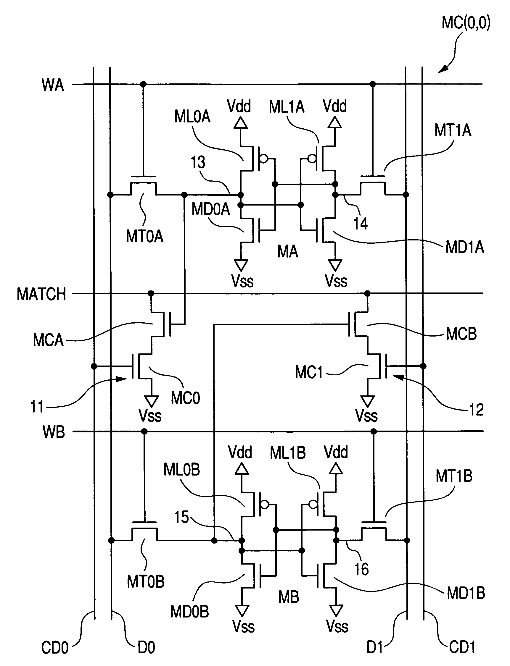
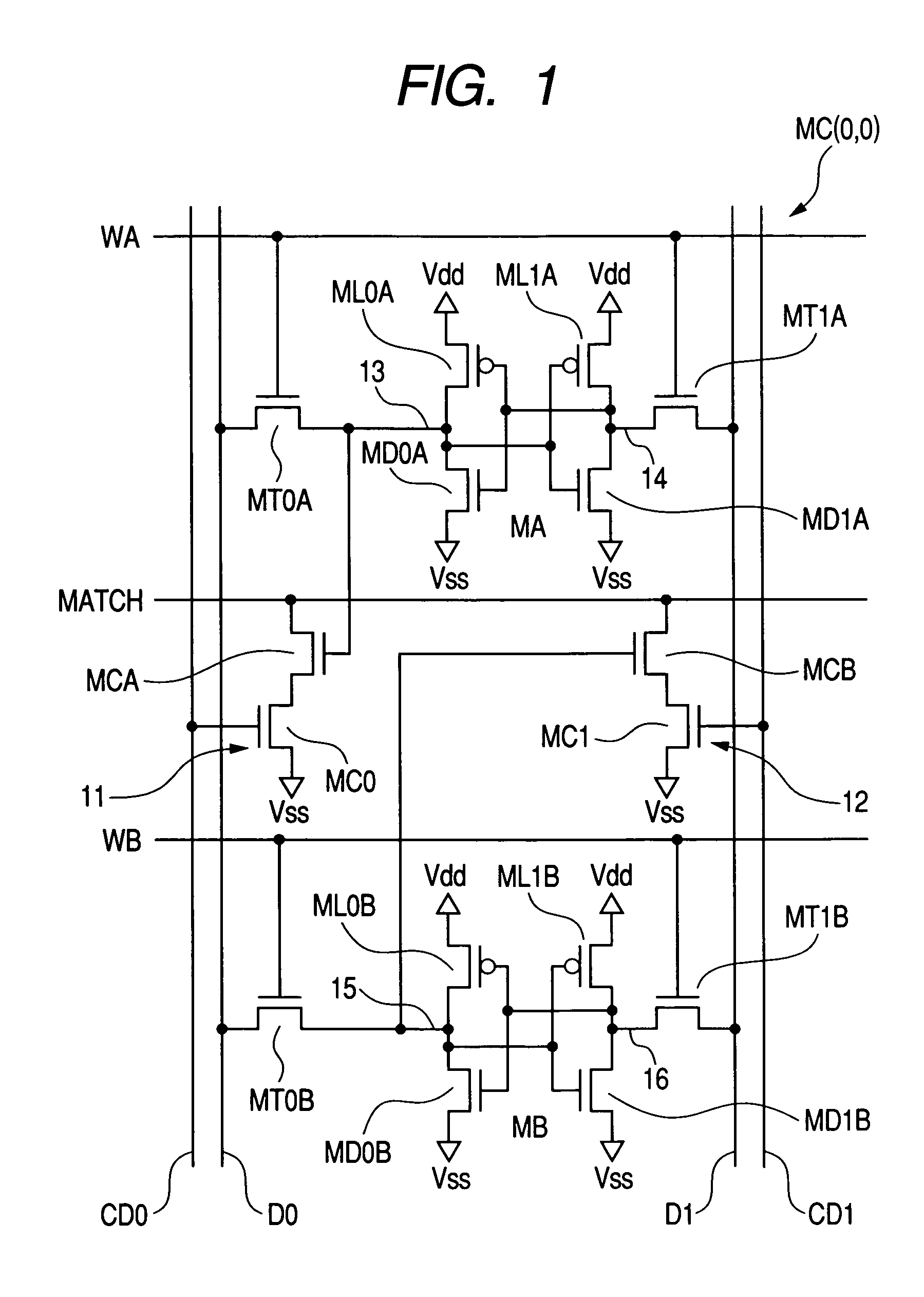
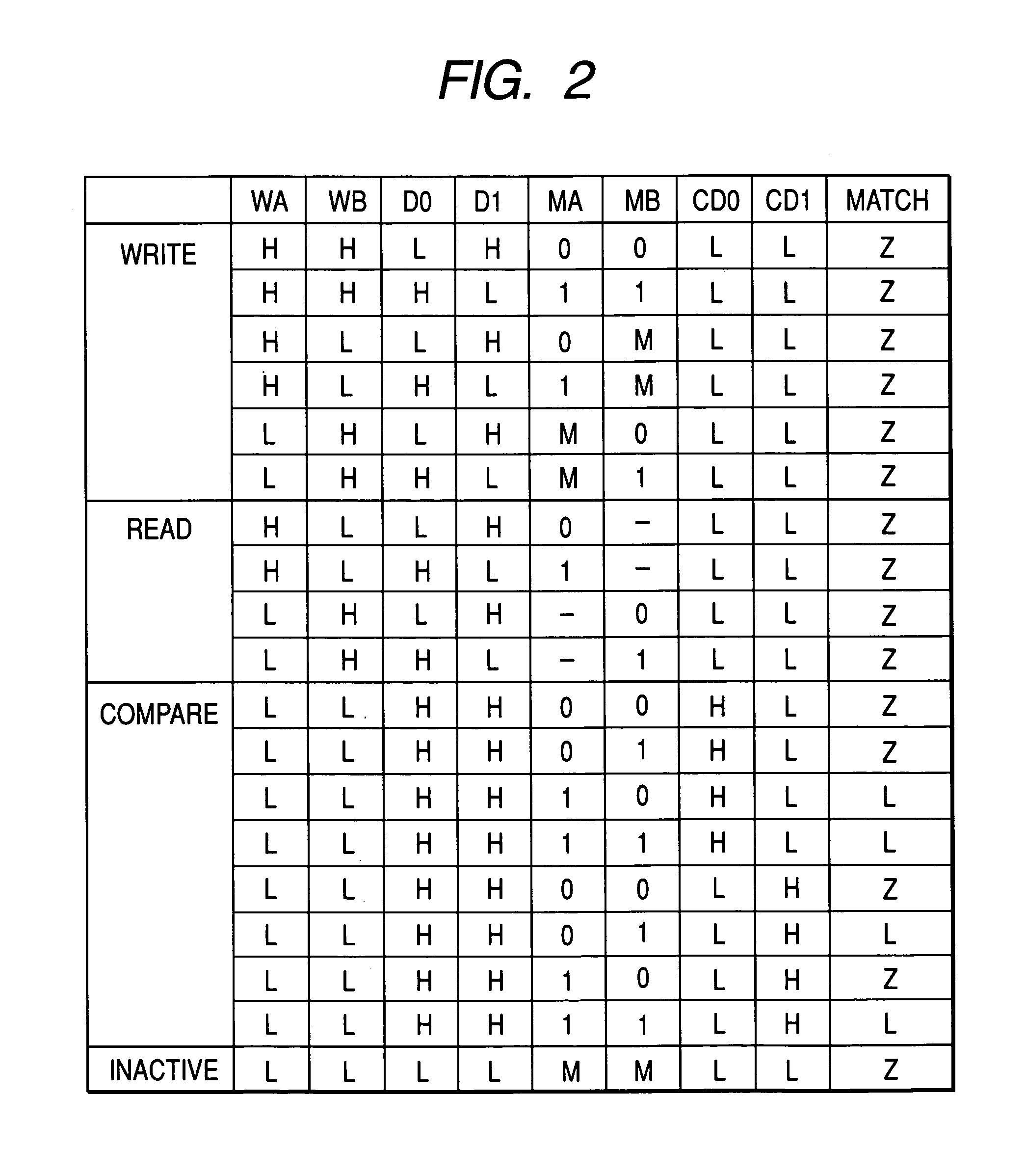
[0045]FIG. 20 shows an LSI for a router according to an example of a semiconductor device in accordance with the invention. An LSI 200 for a router comprises a routing processor 201 for carrying out a transfer processing for a packet in accordance with destination address information included in packet data according to a predetermined program, an IP address search unit 210 for searching IP address information corresponding to a destination address transmitted from the routing processor 201 by using a routing table, and a routing information output portion 220 for outputting routing information corresponding to the IP address information searched by the IP address search unit 210, and is formed on one semiconductor substrate such as a monocrystalline silicon substrate by a well-known semiconductor integrated circuit manufacturing technique. The routing processor 201 carries out a transfer processing for packet data in accordance with the routing information transmitted from the rout...


PUM


Abstract

Data lines (D0, D1) are shared by a first storage portion (MA) and a second storage portion (MB), and furthermore, a first transistor (MC0) coupled to a first comparison data portion (CD0) and a second transistor (MCA) coupled to the storage node of a first storage portion are connected in series to form a first comparing circuit (11), and a third transistor (MC1) coupled to a second comparison data line (CD1) and a fourth transistor (MCB) coupled to the storage node of the second storage portion are connected in series to form a second comparing circuit (12). Consequently, it is possible to enhance a symmetry in the layout of a diffusion layer and a wiring layer and to achieve the easiness of a layout in which a memory cell is line symmetrical with respect to a center line passing through a center thereof. Thus, a manufacturing process condition can easily be optimized and a variation in a manufacturing process can be reduced so that the microfabrication of the memory cell can be achieved.

Description

CLAIM OF PRIORITY[0001]The present application claims priority from Japanese application JP2004-000316 filed on Jan. 5, 2004, the content of which is hereby incorporated by reference into this application.FIELD OF THE INVENTION[0002]The present invention relates to a semiconductor device including a content addressable memory (hereinafter referred to as a “CAM”) and more particularly to a layout technique therein, for example, an effective technique which is applied to an LSI for a router.BACKGROUND OF THE INVENTION[0003]With the development of the microfabrication of a semiconductor integrated circuit, the exposure light wavelength of a photolithography equipment has been shortened from a g-line to an i-line, and furthermore, an excimer laser. However, a requirement for the microfabrication has been given earlier than a progress in a reduction in the wavelength of the equipment, and in recent years, it has been necessary to reduce a pattern dimension to be equal to or smaller than ...

Claims


Application Information

Patent Timeline
Patent Type & Authority Patents(United States)
IPC IPC(8): G11C7/00G11C15/04G11C16/04H01L21/8244H01L27/11
CPCG11C15/04H01L27/1104H01L27/11G11C15/043H10B10/00H10B10/12
Inventor HIGETA, KEIICHIIWAHASHI, SATOSHIAIHARA, YOICHIRONAKAHARA, SHIGERU
Owner HITACHI LTD
Why Eureka
Try Eureka