
Light absorbent agent polymer for organic anti-reflective coating and preparation method and organic anti-reflective coating composition comprising the same

a technology of light absorbent agent and organic anti-reflective coating, which is applied in the direction of photosensitive materials, instruments, photomechanical equipment, etc., can solve the problems of cd (critical dimension) alteration, affecting the processing of photoresist, and standing waves and reflective notching inevitably occur

Inactive Publication Date: 2006-04-25
SK HYNIX INC
View PDF4 Cites 61 Cited by
  • Summary
  • Abstract
  • Description
  • Claims
  • Application Information

AI Technical Summary

Benefits of technology

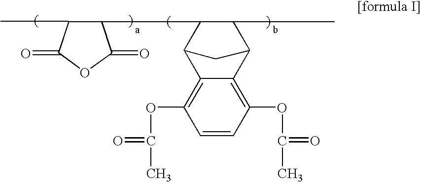
[0022]The polymer of formula I contains chromophore having a high absorbance at the wavelength of 193 nm, and comprises maleic anhydride as a monomer status to sufficiently form a cross-linkage bond with a cross-linking polymer having an acetal functional group. Because of such characteristics, the polymer of formula I can be preferably used as the light absorbent agent in the organic anti-reflective coating composition with respect to the light source having 193 nm wavelength. That is, since the polymer of formula I is included in the coating composition for serving as the light absorbing agent, it can control the light interference phenomenon during the ultra-fine pattern formation process using the 193 nm light source. In addition, the polymer can easily form the cross-linkage bond with the cross-linking polymer to give solvent-resistant ability to the anti-reflective coating, thereby ensuring improved photoresist patterns by employing the coating composition containing such light absorbent agent to form the anti-reflective coating.
[0031]Briefly, the above coating composition of the present invention comprises the polymer represented by the formula I as the light absorbent agent, in which the maleic anhydride group contained in the polymer of formula I can generate the cross-linkage bond with the acetal functional group contained in the cross-linking polymer of formula II, whereby the formed anti-reflective coating has the solvent-resistance. Also, by such cross-linkage bond, it is possible to protect chemical materials such as acid or amine from being transferred out of the anti-reflective coating, in turn, to minimize under-cutting and / or putting phenomenon to result in formation of the improved photoresist pattern. Furthermore, both of the polymers represented by the formulae I and II comprise a chromophore having a remarkably high absorbance to absorb light reflected or diffused at bottom portion of the photoresist film and to remarkably reduce standing wave effect caused by such reflected and / or diffused light.
[0039]The thermal acid generator serves as a catalyst for activating such cross-linking reaction between the above cross-linking agent and the light absorbent agent. When a thermal process such as the baking process is carried out after applying such thermal acid generator on a wafer, acid is generated from the thermal acid generator and, in the presence of acid generated by the above process, the cross-linking reaction brings out to form the organic anti-reflective coating insoluble in the solvent for the photoresist. In other words, it is possible to accelerate the cross-linking reaction between the light absorbent agent and the cross-linking agent by employing the compound of the formula VII as the thermal acid generator.
[0042]Therefore, when a baking process is carried out after applying the organic anti-reflective coating composition comprising such components mentioned as above with the composition rates, acid is generated from the thermal acid generator and, the cross-linking reaction brings out between the light absorbent agent polymer of formula I and the cross-linking agent polymer of formula II by the acid generated from the above process to form the organic anti-reflective coating. Such organic anti-reflective coating can absorb far-infrared ray transmitting the photoresist film and reaching to the organic anti-reflective coating, thereby preventing diffused light reflection from the bottom layer of the photoresist film.

Problems solved by technology

In a fabrication process of ultrafine patterns for preparing semiconductor devices, standing waves and reflective notching inevitably occur due to the optical properties of lower film layer on the photoresist film and due to thickness changes in the photosensitive film.
In addition, there is another problem in that a CD (critical dimension) alteration is caused by diffracted and reflected light from the lower film layers.
Such anti-reflective coating can absorb the scattered and / or reflected light and, thereby, directly affecting the processing of the photoresist.
However, in an ultra-fine pattern forming process using ArF light (193 nm), no proper anti-reflective coating has been developed yet.
Especially, in the case of an inorganic anti-reflective coating, no material is known which enables the control of the interference at 193 nm, the wavelength of the light source.

Method used


Image

  • Light absorbent agent polymer for organic anti-reflective coating and preparation method and organic anti-reflective coating composition comprising the same
  • Light absorbent agent polymer for organic anti-reflective coating and preparation method and organic anti-reflective coating composition comprising the same
  • Light absorbent agent polymer for organic anti-reflective coating and preparation method and organic anti-reflective coating composition comprising the same

Examples


example 1

[0052]Preparation of light absorbent agent polymer

[0053]20 g of maleic anhydride and 26 g of 1,4-dihydro-1,4-methanonaphthalene-5,8-diol diacetate (0.5% by mole per maleic anhydride) were dissolved in 26 g of PGMEA solvent. The dissolved mixture was added with 0.5 g of AIBN to form a vacuum condition and then reacted at 65° C. for 7 hours. After completing the reaction, the solvent was removed from the obtained solution by means of an evaporator. Thereafter, the treated solution was under deposition and filtration processes in distilled water, then washed by using ethylether several times to produce the light absorbent agent polymer of formula I (yield 40%).

[0054]Molecular weight: 7,000

example 2

[0055]Preparation of organic anti-reflective coating composition

[0056]1 g of the light absorbent agent polymer prepared from Example 1 and 0.4 g of the cross-linking agent polymer of formula III were dissolved in a solvent mixture comprising 4 g of propylene glycol methylether acetate solvent; log of methyl 3-methoxy propionate solvent; 10 g of 2-heptanone solvent; and 7 g of tetrahydrofurane solvent. After adding 0.1 g of the thermal acid generator having the structure represented by formula VII to the resultant material to be dissolved, the dissolved mixture passed through a filter to produce the desired organic anti-reflective coating composition.

[0057]

example 3

[0058]Formation of organic anti-reflective coating and photoresist pattern

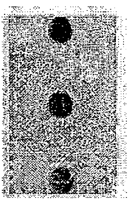
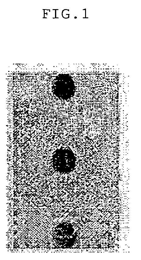
[0059]On a silicone wafer, a spin-coating was carried out with the organic anti-reflective coating composition prepared in Example 2, then a baking process was conducted for the obtained material at 215° C. for 2 minutes to generate the cross-linkage bond to form the desirable anti-reflective coating. Thereafter, the obtained anti-reflective coating was under a coating process with a so-called Keum Ho petroleum photosensitive agent (the name generally used for photoresist materials) and another baking process at 110° C. for 90 seconds. After conducting the above baking process, the baked product was exposed to a light source by means of ASML / 900 scanner apparatus, then, under an additional baking process at 130° C. for 90 seconds. The exposed wafer was developed by using an aqueous solution of 2.38% by weight of TMAH. From the developed material, produced was the pattern shown in FIG. 1.

[0060]As mentioned abov...


PUM

PropertyMeasurementUnit
thicknessaaaaaaaaaa
wavelengthaaaaaaaaaa

Abstract

Disclosed are a light absorbent agent polymer for organic anti-reflective coating which can prevent diffused reflection of lower film layer or substrate and reduce standing waves caused by variation of thickness of the photoresist itself, thereby, increasing uniformity of the photoresist pattern, in a process for forming ultra-fine patterns of photoresist for photolithography by using 193 nm ArF among processes for manufacturing semiconductor device, and its preparation method. Also, the present invention discloses an organic anti-reflective coating composition comprising the light absorbent agent polymer for the organic anti-reflective coating and a pattern formation process using the coating composition.

Description

BACKGROUND OF THE INVENTION[0001]1. Field of the Invention[0002]The present invention relates to a light absorbent agent polymer for an organic anti-reflective coating which can prevent diffused reflection of the lower film layer or substrate and reduce standing waves caused by variation in the thickness of the photoresist itself, thereby, increasing uniformity of the photoresist pattern, in a process for forming ultra-fine patterns of photoresist for photolithography by using 193 nm ArF among processes for manufacturing semiconductor device, and its preparation method.[0003]Also, the present invention provides an organic anti-reflective coating composition (hereinafter abbreviated as “the coating composition”) comprising the light absorbent agent polymer for the organic anti-reflective coating (hereinafter abbreviated as “the coating polymer”) and a pattern formation process using the coating composition.[0004]2. Description of the Related Art[0005]In a fabrication process of ultra...

Claims


Application Information

Patent Timeline
Patent Type & Authority Patents(United States)
IPC IPC(8): G03C1/73C08F34/02G03C1/835G03F7/20G03F7/36C08F232/08G03F7/039G03F7/09
CPCC08F232/08G03F7/091Y10S430/126Y10S430/106Y10S430/122G03F7/039
Inventor JUNG, JAE-CHANGKONG, KEUN KYUKIM, SEOK-KYUN
Owner SK HYNIX INC
Learn More