Surface treatment using iodine plasma to improve metal deposition

a surface treatment and metal deposition technology, applied in the field of chemical vapor deposition of metal, can solve the problems of difficult physical vapor deposition to line holes and trenches with uniform and conformal thin films of integrated circuit materials, ruthenium and ruthenium, and physical vapor deposition techniques are often unsatisfactory for obtaining good quality, continuous, conformal thin films, etc., to reduce the time required for metal nucleation and improve metal deposition

Active Publication Date: 2006-05-09
NOVELLUS SYSTEMS
View PDF16 Cites 22 Cited by
  • Summary
  • Abstract
  • Description
  • Claims
  • Application Information

AI Technical Summary

Benefits of technology

[0021]A method in accordance with the invention improves metal deposition on an integrated circuit substrate. Plasma treatment of a substrate surface in accordance with the invention usually reduces the time required for nucleation of metal on the substrate surface during a chemical vapor deposition process, thereby decreasing the nucleation delay of metal growth on the substrate surface. Improved nucleation of metal resulting from plasma treatment in accordance with the invention improves surface morphology of deposited metal, allowing thinner films to be continuous. Further, plasma treatment in accordance with the invention generally decreases the deposition rate of metal onto the plasma-treated surface, thereby improving control of the growth and thickness of metal films, especially ultra-thin films. It is believed that plasma treatment of a surface with excited species (e.g., excited iodine species) in accordance with the invention suppresses the subsequent deposition rate of ruthenium or other metal on the treated surface, resulting in less “island” growth and more uniform layer growth. Plasma treatment of a substrate surface in accordance with the invention improves adhesion of deposited metal to the substrate surface. Improved morphology and greater smoothness of metal deposited in accordance with the invention improves adhesion of materials subsequently formed in contact with the metal. As a result, overall film-stack adhesion is enhanced. Also, thinner barrier layers, electrodes, wiring layers and other metal-containing conductive and nonconductive layers can be deposited on dielectric layers in integrated circuit substrates without necessarily first forming a metal seed layer.

Problems solved by technology

As the design density of integrated circuits increases, resulting in smaller dimensions of holes and trenches, it is generally more difficult to use physical vapor deposition to line holes and trenches with uniform and conformal thin films of integrated circuit material.
As the design density of integrated circuits increases, resulting in smaller design features and dimensions, deposition of ruthenium and ruthenium oxide thin films, as well as thin films of other materials, by physical vapor deposition techniques is often unsatisfactory for obtaining good quality, continuous, and conformal thin films.
Chemical vapor deposition of metal directly onto a dielectric material, such as silicon oxide, SiO2, or onto standard adhesion layer material, such as tantalum nitride, TaN, is often accompanied by delayed and discontinuous growth, surface roughness and poor adhesion.
These problems are especially acute in processes for depositing ruthenium on silicon oxide (SiO2) without a seed layer.
Many other metal CVD processes, for example, MOCVD of copper, suffer these problems also.
Adsorption of iodine and some other surfactants onto less-reactive surfaces, such as TiN, TaN and other metal nitrides used for diffusion barriers, and particularly onto nonmetal dielectric surfaces (e.g., SiO2), however, has not been demonstrated to achieve good thin film morphology of ruthenium and of some other metals.
The chemical vapor deposition of metal films on dielectric substrates is often difficult due to the inability of the metal to nucleate on dielectric surface.
This leads to long process times, poor adhesion and surface roughness.
The deposition of a metal thin film, particularly of ruthenium, Ru, or other Ru-containing layer by chemical vapor deposition (such as MOCVD and ALD) without a metal seed layer often results in poor morphology of the thin film.

Method used


Image

  • Surface treatment using iodine plasma to improve metal deposition
  • Surface treatment using iodine plasma to improve metal deposition
  • Surface treatment using iodine plasma to improve metal deposition

Examples


example 1

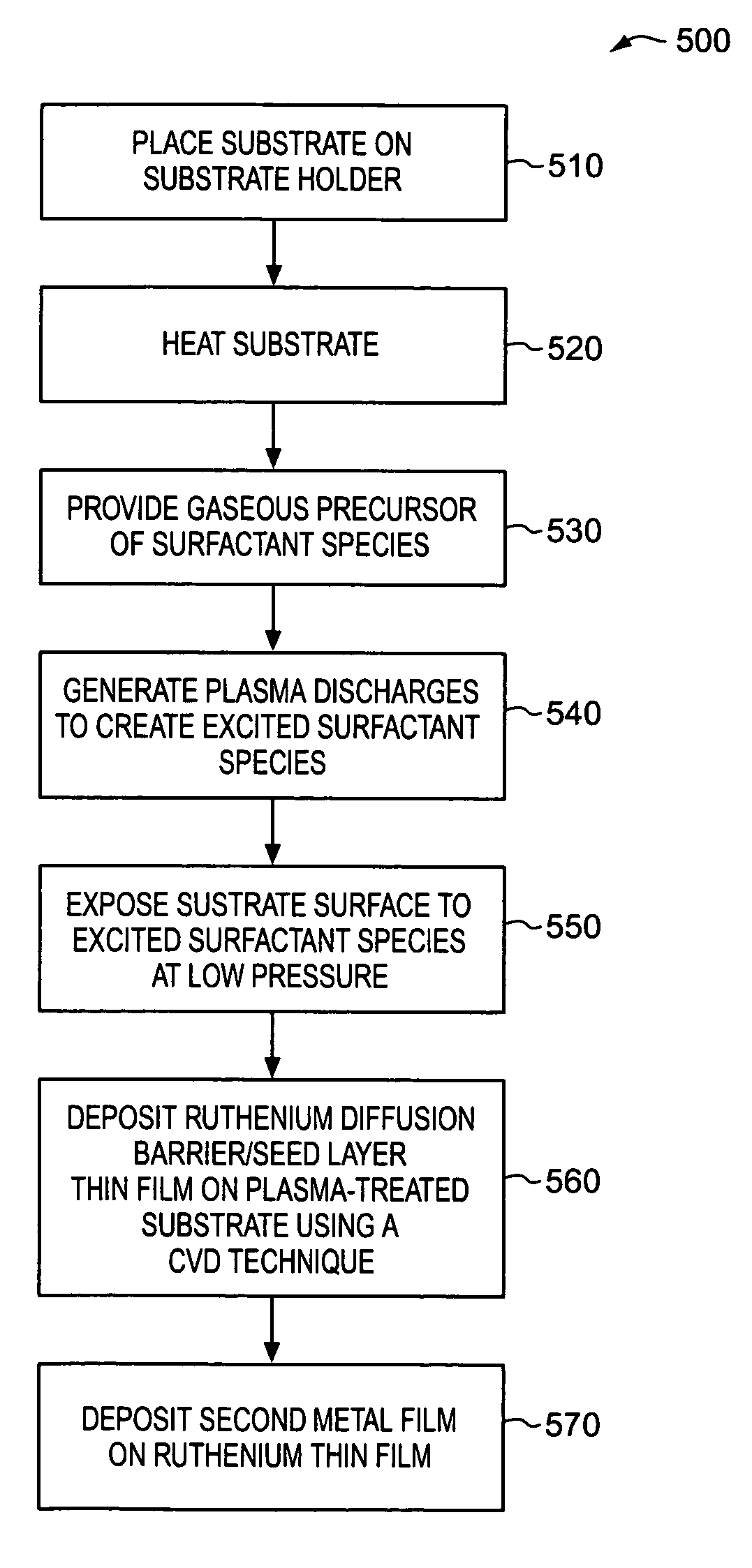
[0077]A series of 200 mm silicon semiconductor wafers having a thermal silicon dioxide, SiO2, substrate surface were plasma-treated in accordance with the invention. Each untreated wafer was placed on a heated substrate holder in vacuum chamber having an internal free volume of approximately 20 liters. The pressure of the chamber was maintained at about 300 mTorr. The wafer was heated to a temperature in a range of about from 300° C. to 360° C. Argon gas was flowed continuously via an inlet showerhead through the vacuum chamber at flow rate of about 250 sccm. A dose of ethyliodine (C2H5I) surfactant precursor gas having a volume of 25 cc at 157 Torr pressure was flowed during a treatment time of approximately 20 seconds at an approximately uniform flowrate (i.e., about 15 sccm ethyliodine) into the inlet showerhead, where it mixed with the argon gas and the mixture flowed into the vacuum chamber. During the 20-second treatment time, 300 W HF-RF power was applied at 13.56 MHz to the ...

example 2

[0081]A series of 200 mm silicon semiconductor wafers having a thermal silicon dioxide, SiO2, substrate surface were plasma-treated in accordance with the invention as in Example 1.

[0082]After plasma treatment, a conventional ALD technique was conducted to deposit a thin film of ruthenium metal, Ru, on each of several treated wafers. The ALD technique was conducted on different wafers at one of two different temperatures in the reaction chamber, 330° C. and 360° C. The ALD technique was varied between wafers by varying the total number of ALD deposition cycles conducted with a given wafer. The total number of ALD deposition cycles was repeated up to three hundred times to deposit a thin film of ruthenium. The MOCVD apparatus used in Example 1 was modified for the ALD processes.

[0083]The conventional ALD deposition cycle used included four stages: a ruthenium-containing precursor dosage; a first, post-precursor inert-gas purge stage; a surface-reactivation stage, in which an oxidizin...


PUM

PropertyMeasurementUnit
thicknessaaaaaaaaaa
thicknessaaaaaaaaaa
thicknessaaaaaaaaaa

Abstract

An excited surfactant species is created by generating plasma discharge in a surfactant precursor gas. A surfactant species typically includes at least one of iodine, led, thin, gallium, and indium. A surface of an integrated circuit substrate is exposed to the excited surfactant species to form a plasma-treated surface. A ruthenium thin film is deposited on the plasma-treated surface using a CVD technique.

Description

FIELD OF THE INVENTION[0001]The invention is related to the field of chemical vapor deposition of metal in integrated circuit fabrication, in particular to methods for treating an integrated circuit substrate to promote MOCVD or ALD of ruthenium and other metals.BACKGROUND OF THE INVENTION[0002]The chemical vapor deposition of metal and metal-containing films on dielectric substrates is of great interest in many areas of semiconductor fabrication, such as deposition of metal wiring, electrodes, and diffusion barriers. In particular, thin films of ruthenium, Ru, and ruthenium oxide, RuO2, are useful in integrated circuit devices and in fabrication of integrated circuits. Ruthenium and ruthenium oxide are generally useful as electrical contact materials. They have good electrical conductivity and show good environmental stability. They are useful for contact metallizations, diffusion barriers, and gate metallizations. Ruthenium oxide electrodes have also shown utility as working elect...

Claims


Application Information

Patent Timeline
Patent Type & Authority Patents(United States)
IPC IPC(8): H01L21/4763
CPCC23C16/0245C23C16/18H01L21/28556H01L21/28562H01L21/76877H01L21/76826H01L21/76843H01L21/76873H01L21/76802
Inventor DALTON, JEREMIE JAMESGOPINATH, SANJAYBLACKBURN, JASON M.DREWERY, JOHN STEPHEN
Owner NOVELLUS SYSTEMS
Why Eureka
Try Eureka