
Method for fabricating ferroelectric random access memory device

Inactive Publication Date: 2006-05-16
SK HYNIX INC
View PDF6 Cites 11 Cited by
  • Summary
  • Abstract
  • Description
  • Claims
  • Application Information

AI Technical Summary

Benefits of technology

[0024]It is, therefore, an object of the present invention to provide a method for fabricating a ferroelectric random access memory (FeRAM) device capable of preventing oxidation of a barrier metal layer of a storage node contact due to oxygen diffused along an interface between a bottom electrode and an inter-layer insulation layer during a high thermal process.
[0025]It is another object of the present invention to provide a method for fabricating a FeRAM device capable of solving a problem of an insufficient process margin caused by an additional masking and etching process for opening a portion of an adhesion layer formed above an upper part of a tungsten plug.

Problems solved by technology

However, such noble metal used as the bottom electrode has a weak adhesion with an inter-layer insulation layer, especially an oxide layer.
Thus, during a subsequent dielectric layer deposition process, a thermal process and a cleaning process, there occurs a lifting phenomenon between the inter-layer insulation layer and the bottom electrode, further resulting in structural deformation, which impedes effective fabrication of semiconductor devices.
The above described method is disadvantageous by requiring an additional process for etching the adhesion layer 22 to make the upper part of the tungsten plug 20A be exposed.
Also, as a semiconductor device has become highly integrated, there is not a sufficient margin for the etching process for etching the adhesion layer 22 with respect to the bottom electrode.
The oxidation of the third titanium nitride layer may increase leakage currents.
As described above, in the conventional method, there may not be a sufficient process margin for the masking and etching process for opening the predetermined portion of the adhesion layer.
As a result, the oxidated titanium nitride layer may become a negative factor for increasing leakage currents, which in turn, increase the contact resistance between the bottom electrode and the tungsten plug contained in the resulted device.

Method used


Image

  • Method for fabricating ferroelectric random access memory device
  • Method for fabricating ferroelectric random access memory device
  • Method for fabricating ferroelectric random access memory device

Examples


Embodiment Construction

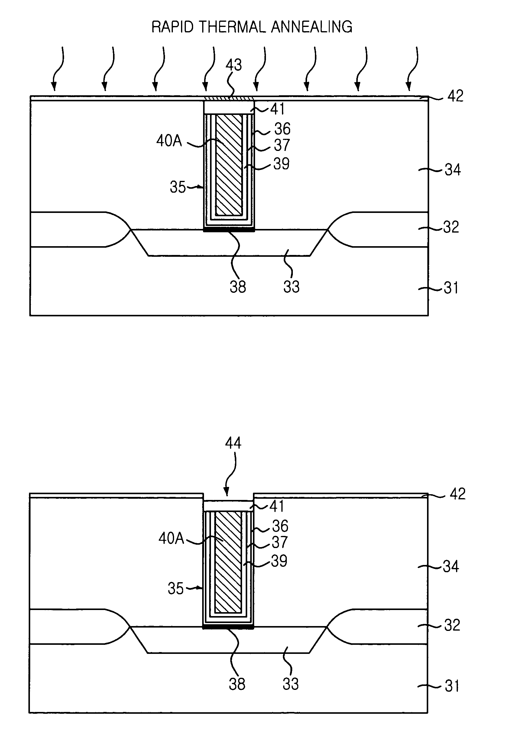
[0037]Hereinafter, variously applicable preferred embodiments of the present invention will be described in detail with reference to the accompanying drawings.

[0038]FIGS. 4A to 4G are cross-sectional views illustrating a method for fabricating a ferroelectric random access memory (FeRAM) device in accordance with a first preferred embodiment of the present invention.

[0039]Referring to FIG. 4A, field oxide layers 32 are formed in a substrate 31, and an impurity junction region 33 such as a source / drain region of a transistor is formed in the substrate 31. Then, a first inter-layer insulation layer 34 is formed on the substrate 31. At this time, the first inter-layer insulation layer 34 has a multi-layer structure to insulate a word line, a landing plug and a bit line before forming a storage node contact. Preferably, the first inter-layer insulation layer 34 is made of a material selected from a silicon oxide group consisting of high density plasma (HDP) oxide, borophosphosilicate gl...


PUM


Abstract

The present invention relates to a method for fabricating a ferroelectric random access memory device. The method includes the steps of: (a) forming a first inter-layer insulation layer on a substrate providing a transistor; (b) etching the first inter-layer insulation layer to form a storage node contact hole exposing a partial portion of the substrate; (c) burying a storage node contact including a plug and a barrier metal layer into the storage node contact hole; (d) forming an adhesion layer on the storage node contact and the first inter-layer insulation layer; (e) inducing a predetermined portion of the adhesion layer to be cracked, the predetermined portion disposed above an upper part of the plug; (f) selectively removing the cracked predetermined portion to expose a surface of the barrier metal layer formed on the plug; and (g) forming a ferroelectric capacitor connected to the plug through the exposed surface of the barrier metal layer.

Description

FIELD OF THE INVENTION[0001]The present invention relates to a method for fabricating a semiconductor device; and, more particularly, to a method for fabricating a ferroelectric random access memory (FeRAM) device.DESCRIPTION OF RELATED ARTS[0002]It has been continuously attempted to develop a semiconductor memory device capable of operating a large scale of memory size and overcoming a limitation in refresh required by a dynamic random access memory (DRAM) device by employing a ferroelectric thin layer for a ferroelectric capacitor. Such a ferroelectric random access memory (FeRAM) device using the ferroelectric thin layer is a nonvolatile memory device. That is, the FeRAM device has an advantage of retrieving stored information even if the power is turned off. Also, the FeRAM device has been recently highlighted as one of the next generation memory devices by having a compatible operation speed to a DRAM device.[0003]For an upper electrode and a bottom electrode of the ferroelectr...

Claims


Application Information

Patent Timeline
IPC IPC(8): H01B13/00H01L21/00B44C1/22G11C11/22H01L21/02H01L21/306H01L21/469H01L21/768H01L21/82
CPCH01L21/76828H01L21/76829H01L21/76834H01L28/65H01L21/7687H01L21/76877H01L21/76889H01L28/55H01L21/76846H01L21/02052
Inventor KWEON, SOON-YONGYEOM, SEUNG-JIN
Owner SK HYNIX INC
Features
  • Generate Ideas
  • Intellectual Property
  • Life Sciences
  • Materials
  • Tech Scout
  • Unparalleled Data Quality
  • Higher Quality Content
  • 60% Fewer Hallucinations
Learn More