

Metal plating method, pretreatment agent, and semiconductor wafer and semiconductor device obtained using these
a technology of metal ions and pretreatment agents, which is applied in the direction of liquid/solution decomposition chemical coatings, coatings, printed circuit manufacturing, etc., can solve the problems of difficult to obtain a strongly adhered and uniform deposit, complex treatment process, and inability to deposited noble metal ions with adequate efficiency
- Summary
- Abstract
- Description
- Claims
- Application Information
AI Technical Summary
Benefits of technology
Problems solved by technology
Method used
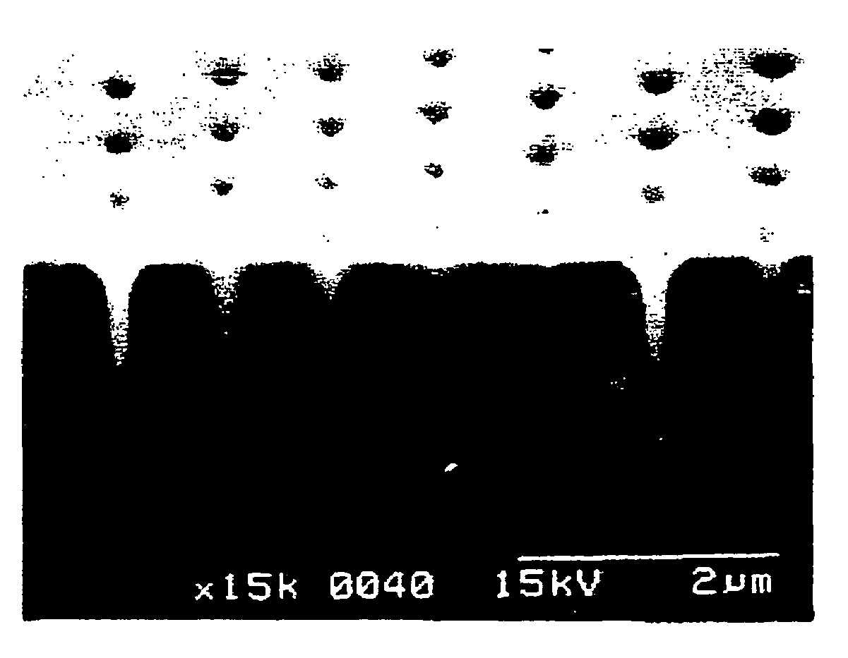
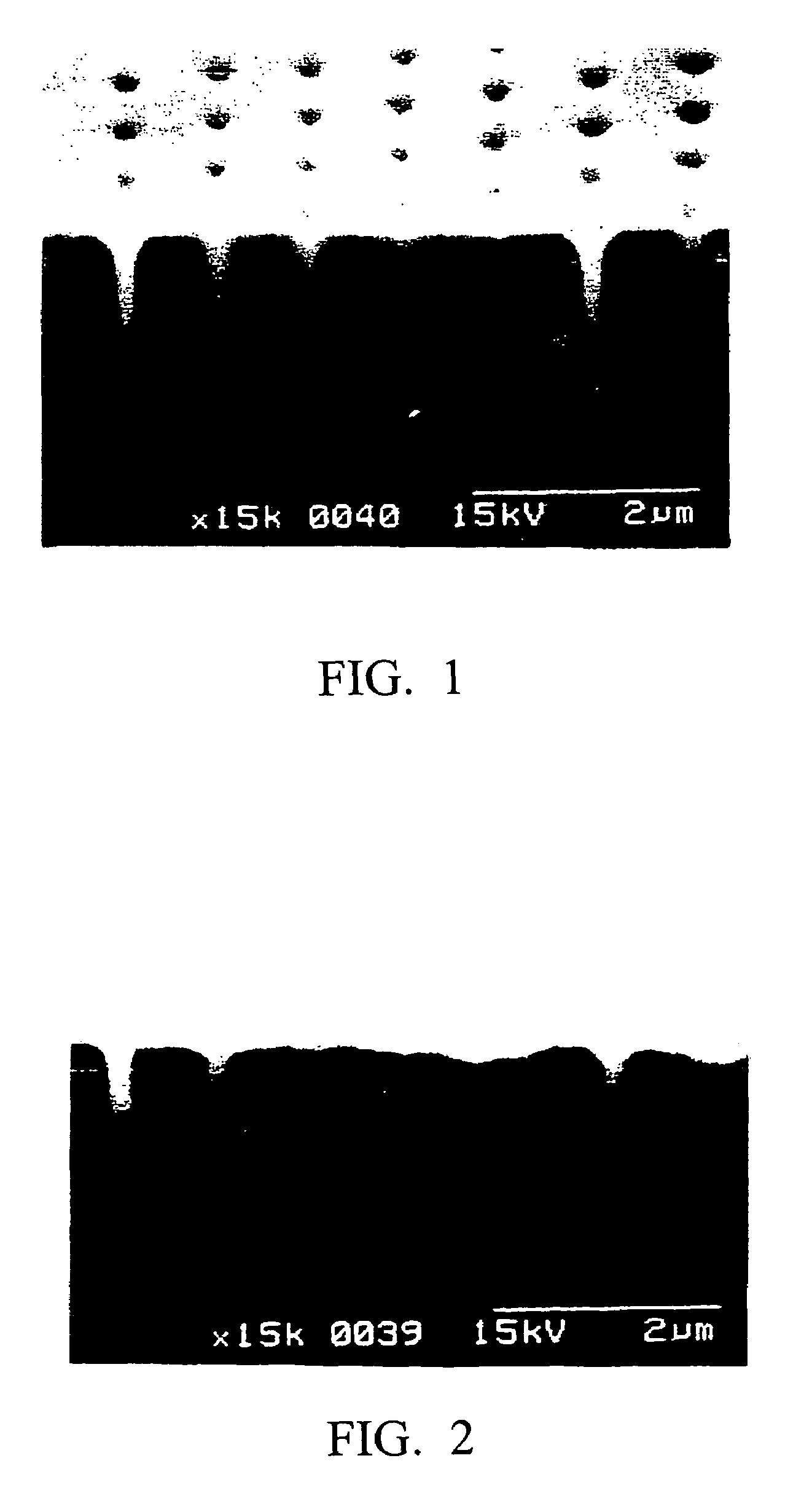
Image

Examples
example 1
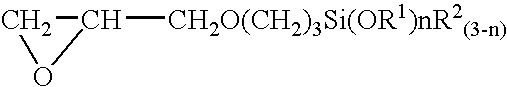
[0045]An equimolar reaction was first conducted between imidazole and γ-glycidoxypropyltrimethoxysilane, yielding a silane-coupling agent as the product. A palladium chloride aqueous solution was subsequently added at room temperature to an aqueous solution containing 0.2 wt % of this silane-coupling agent to achieve the palladium chloride concentration of 150 mg / L, thereby, a pretreatment plating agent was prepared. The pH of this pretreatment agent was 2.9. Polyester resin in the form of a cloth was immersed in the pretreatment plating agent for 3 minutes at room temperature, and the polyester cloth was then thoroughly rinsed in running water. The polyester cloth was then plated at 70° C. for 5 minutes with the use of an electroless nickel plating solution (nickel plating solution FM-0 manufactured by Nikko Metal Plating). As a result, the polyester cloth was provided with a nickel plating that had adequate adhesive strength and uniformity across the entire surface.
example 2
[0046]Nylon cloth was immersed for 3 minutes at room temperature in the pretreatment plating agent prepared in Example 1, and thoroughly rinsed in running water. The nylon cloth was then plated at 70° C. for 5 minutes with the use of an electroless nickel plating solution (nickel plating solution FM-0 manufactured by Nikko Metal Plating). As a result, the nylon cloth was provided with a nickel plating that had adequate adhesive strength and uniformity across the entire surface.
example 3
[0047]A palladium chloride aqueous solution was added at room temperature to an aqueous solution containing 0.05 wt % of the silane-coupling agent prepared in Example 1 to achieve the palladium chloride concentration of 80 mg / L, thereby, a pretreatment plating agent was prepared. Polyester cloth was immersed in the pretreatment plating agent for 3 minutes at room temperature, and the polyester cloth was then thoroughly rinsed in running water. The polyester cloth was then plated at 70° C. for 5 minutes with the use of an electroless nickel plating solution (nickel plating solution FM-0 manufactured by Nikko Metal Plating). As a result, the polyester cloth was provided with a nickel plating that had adequate adhesive strength and uniformity across the entire surface.
PUM
| Property | Measurement | Unit |
|---|---|---|
| concentration | aaaaa | aaaaa |
| pH | aaaaa | aaaaa |
| volatilization temperature | aaaaa | aaaaa |
Abstract
Description
Claims
Application Information