Symbol-based signaling device for an electromagnetically-coupled bus system

a bus system and signaling device technology, applied in the field of symbolic signaling devices for electromagnetically coupled bus systems, can solve the problems of affecting the performance of the processor, and outperforming the data delivery bandwidth of the conventional system by significant margins,

Inactive Publication Date: 2006-07-11
INTEL CORP
View PDF32 Cites 137 Cited by
  • Summary
  • Abstract
  • Description
  • Claims
  • Application Information

AI Technical Summary

Problems solved by technology

The data throughput of these processors outstrips the data delivery bandwidth of conventional systems by significant margins.
However, even the best caching architecture can leave a processor under-utilized.
Similar problems arise in any digital system, such as communication networks, routers, backplanes, I / O buses, portable device interfaces, etc., in which data must be transferred among devices that operate at ever higher frequencies.
However, these parameters cannot be increased without limit.
Interference between scattered and unscattered signals can significantly reduce signal reliability.
However, impedance matching requires the use of precision components, which increases the costs of these systems.
In addition to impedance discontinuities, connections to bus traces may also affect system performance by adding capacitance.
Capacitance can slow signal propagation speed and lower the trace impedance, which may require larger driver circuits with increased power consumption.
For these systems, devices are mounted on daughter cards, which are connected in series with the bus through costly, tightly matched connectors.
In addition, the different daughter card components must be impedance matched to each other and the connectors, and the parasitic capacitances of these components, all of which touch some portion of the bus, further affect the signal propagation speed, impedance, driver size, and power dissipation.
They can also attenuate the signal energy rapidly, and on multi-drop buses, little signal energy may be available to devices that are farther from the signal source.
On the other hand, coupling coefficients that are too small or lengths that are too short result in low signal to noise ratios at the devices.
Variations in the relative positions can increase noise on the bus trace or reduce the transferred signal relative to non-scalable noise according to whether the distance decreases or increases, respectively.
For example, the greater self-induced noise associated with high frequency signaling limits the reliability with which signals can be resolved.
This limits the opportunity for employing higher symbol densities.
Use of these techniques has been largely limited to point-to-point communication systems, particularly at high signaling frequencies.
Transmission line effects limit the use of modulation in high frequency communications, especially in multi-drop environments.

Method used


Image

  • Symbol-based signaling device for an electromagnetically-coupled bus system
  • Symbol-based signaling device for an electromagnetically-coupled bus system
  • Symbol-based signaling device for an electromagnetically-coupled bus system

Examples


embodiment 500

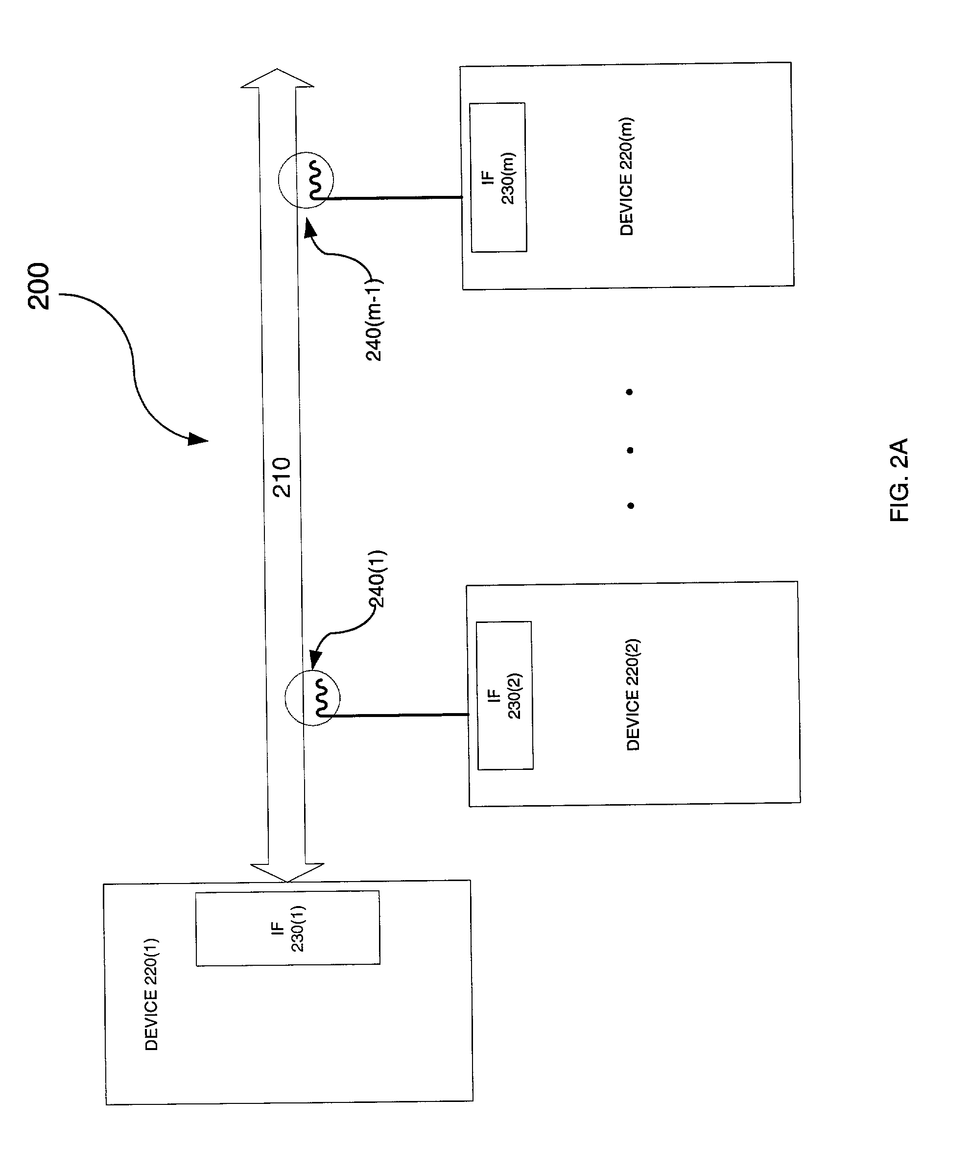
[0074]FIG. 5A is a block diagram of an embodiment 500 of interface 230 suitable for processing multi-bit symbols for devices 220(2)–220(m). For example, interface 500 may be used to encode outbound bits from, e.g., device 220(2) into a corresponding symbol for transmission on bus 210, and to decode a symbol received on bus 210 into inbound bits for use by device 220(2).

[0075]The disclosed embodiment of interface 230 includes a transceiver 510 and a calibration circuit 520. Also shown in FIG. 5A is device side component 242 of electromagnetic coupler 240 to provide a transferred waveform to transceiver 510. For example, the transferred waveform may be the differentiated waveform generated by transmitting pulse 420 across electromagnetic coupler 240. A device side component 242 is provided for each channel, e.g. bus trace, on which interface 230 communicates. A second device side component 242′ is indicated for the case in which differential signaling is employed.

[0076]Transceiver 510...

embodiment 600

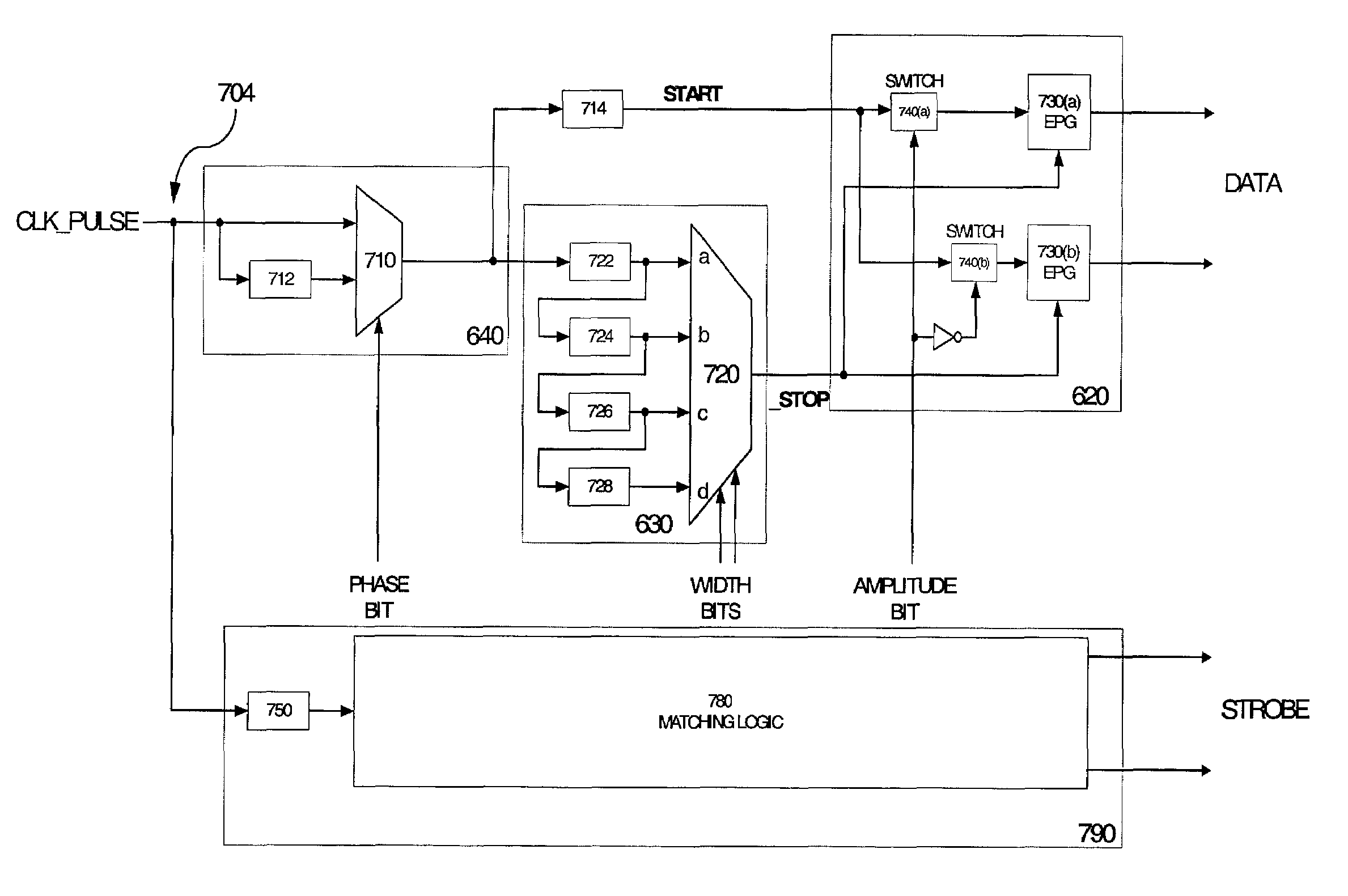
[0079]FIG. 6 is a block level diagram representing an embodiment 600 of transceiver 510 that is suitable for handling waveforms in which data bits are encoded using phase, pulse-width and amplitude modulation, and the strobe is provided by a clock signal. Transceiver 600 supports differential signaling, as indicated by data pads 602, 604, and it receives calibration control signals from, e.g., calibration circuit 520, via control signals 608.

[0080]For the disclosed embodiment of transceiver 510, transmitter 540 includes a phase modulator 640, a pulse-width modulator 630, an amplitude modulator 620 and an output buffer 610. Output buffer 610 provides inverted and non-inverted outputs to pads 602 and 604, respectively, to support differential signaling. A clock signal is provided to phase modulator 640 to synchronize transceiver 510 with a system clock. The disclosed configuration of modulators 620, 630, and 640 is provided only for purposes of illustration. The corresponding modulati...


PUM


Abstract

The present invention provides a chipset for transferring data through an electromagnetically coupled bus system. The chipset includes a modulator, a matching circuit and a demodulator. The modulator modifies a clock to encode multiple bits in a complementary pair of symbols. The matching circuit modifies the clock signal to generate a complementary pair of reference signals that is transmitted with the complementary symbol pair, and the demodulator decodes a second set of bits from selected properties of a complementary pair of transferred symbols.

Description

RELATED PATENT APPLICATIONS[0001]This patent application is a continuation of U.S. patent application Ser. No. 09 / 714,244, now U.S. Pat. No. 6,697,420, entitled “Symbol-Based Signaling Device for an Electromagnetically-Coupled Bus System” and filed on Nov. 15, 2000, which is a continuation-in-part of U.S. patent application Ser. No. 09 / 318,287, now U.S. Pat. No. 6,449,308, entitled “Distribution System” and filed on May 25, 1999.BACKGROUND OF THE INVENTION[0002]1. Technical Field[0003]The present invention relates to mechanisms for communicating digital data, and in particular to mechanisms for communicating digital data in an electromagnetically-coupled bus system.[0004]2. Background Art[0005]Digital electronics systems, such as computers, must move data among their component devices at increasing rates to take full advantage of the higher speeds at which these component devices operate. For example, a computer may include one or more processors that operate at frequencies of a gig...

Claims


Application Information

Patent Timeline
Patent Type & Authority Patents(United States)
IPC IPC(8): H04L27/00H04L25/00G06F13/40G06F13/42H04L25/02H04L25/12H05K1/02H05K1/14H05K3/36
CPCG06F13/4086G06F13/426H04L25/0266H04L25/12H04L25/0268H05K3/361H05K1/14H05K1/0237H05K1/0239H04L25/02
Inventor SIMON, THOMAS D.AMIRTHARAJAH, RAJEEVANMARKETKAR, NANDU J.KNIGHT, JR., THOMAS F.
Owner INTEL CORP
Why Eureka
Try Eureka