
Porous film, composition and manufacturing method, interlayer dielectric film, and semiconductor device

Inactive Publication Date: 2006-08-01
PANASONIC CORP
View PDF8 Cites 13 Cited by
  • Summary
  • Abstract
  • Description
  • Claims
  • Application Information

AI Technical Summary

Benefits of technology

[0023]An object of the invention is to provide a porous film-forming composition from which a porous film having a relative dielectric constant of 2.0 or less and a high mechanical strength can be formed by a practically acceptable process and at a low cost, a method of manufacturing a porous film, a porous film manufactured thereby, and an interlayer dielectric film. Another object is to provide a semiconductor device having a porous film built therein and featuring high performance and high reliability.
[0034]Then, the porous films are minimized in moisture absorption while maintaining mechanical strength for a semiconductor device, so that a semiconductor device having low dielectric constant insulating films built therein is provided. The low dielectric constant of dielectric films ensures to reduce the parasitic capacitance around multilayer interconnects, contributing to a high speed and low power consumption in operation of the semiconductor device.
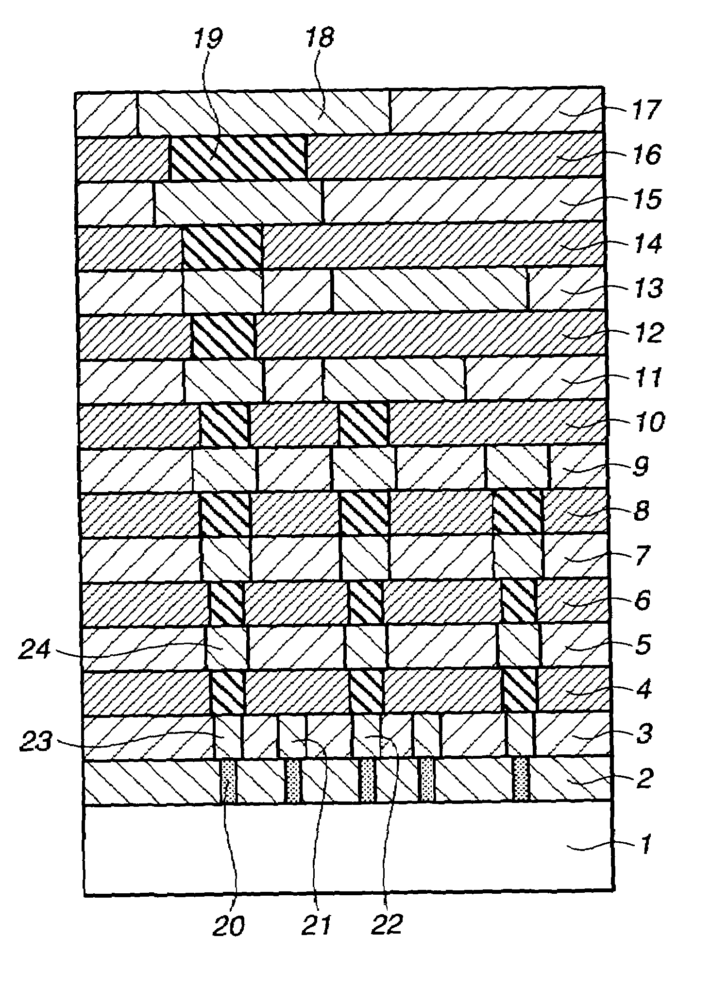
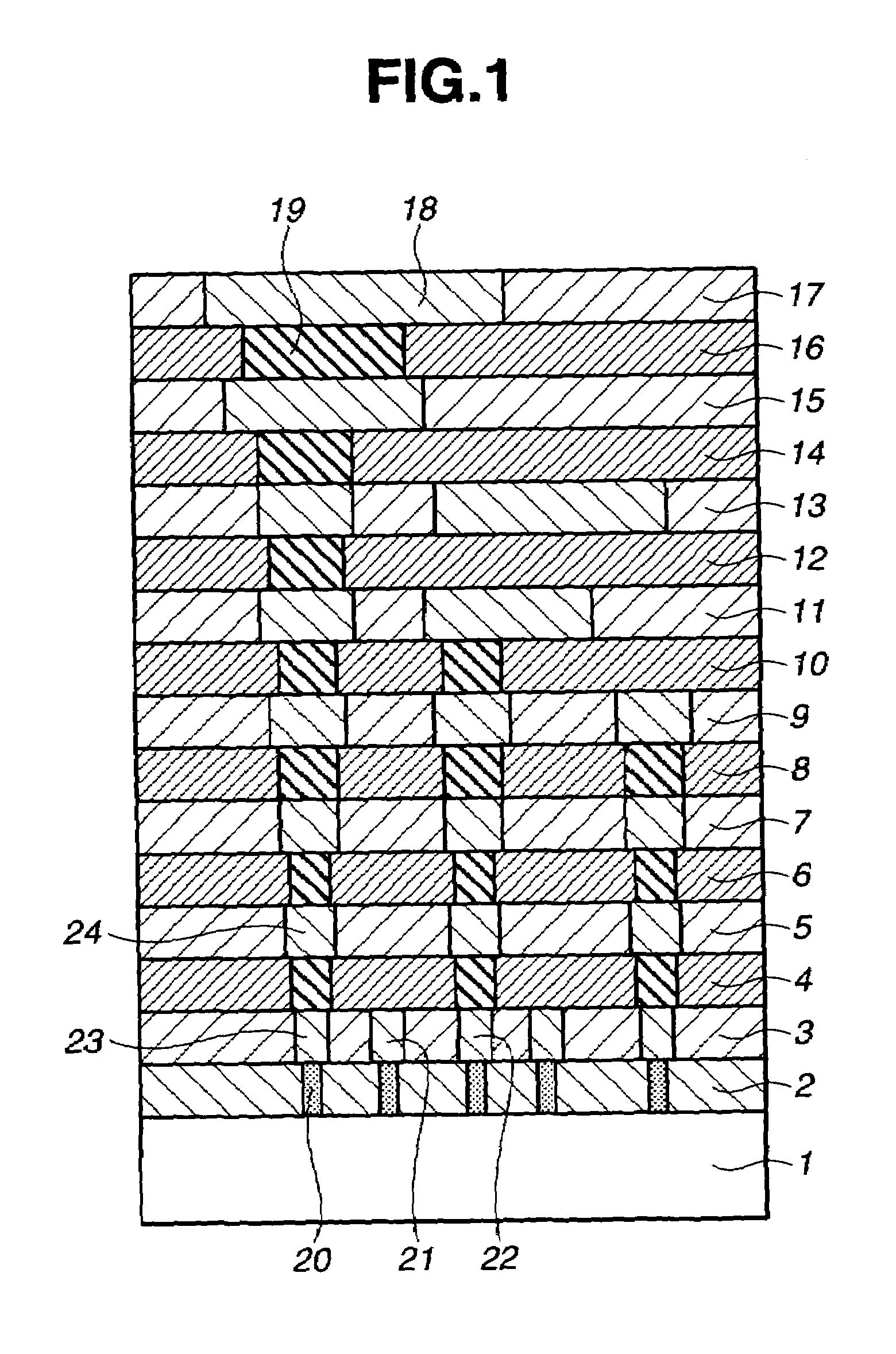
[0035]In a preferred embodiment of the inventive semiconductor device, the porous film is present as a dielectric film between metal wires in an identical layer in a multilayer interconnect structure or as an interlayer dielectric film between upper and lower metal wiring layers. A semiconductor device featuring high performance and high reliability is then provided.

Problems solved by technology

In the progress of semiconductor integrated circuits toward higher integration, an increase of interconnect delay time caused by an increase of wiring capacitance which is a parasitic capacitance between metal wires becomes a barrier in enhancing the performance of semiconductor integrated circuits.
These methods, however, have notable drawbacks.
The first porous film forming method suffers from an increased cost because a siloxane polymer precursor solution must be synthesized.
Additionally, since the precursor solution is applied to form a coating, an amount of silanol groups remain in the coating, which gives rise to a degassing phenomenon that moisture or the like evaporates in the subsequent heat treatment step.
The porous film can be deteriorated in quality by moisture absorption.
The second porous film forming method needs a special applicator apparatus capable of controlling the rate of evaporation of a solvent from a wet gel, adding to the cost.
Since more silanol is left on surfaces of pores, the film as such is hygroscopic and susceptible to substantial quality deterioration.
Thus surface silanol must be silylated, which complicates the process.
In case a wet gel is formed by the CVD process, a special CVD system which is different from plasma CVD systems customarily used in the semiconductor process is needed, adding to the cost as well.
It is then difficult for the porous film to have a relative dielectric constant of 2.0 or less.
Undesirably, component (B) complicates not only the composition, but also the manufacturing process, and increases the cost.
For all these methods, a lowering of mechanical strength of porous films themselves is a problem.
If the silica skeleton has not been densified at this point, the film can be collapsed during the surfactant removal step, failing to effectively introduce pores.
As mentioned above, prior art materials suffer from problems such as the deterioration of film quality by heat treatment and increased costs.
Another problem is the difficulty to reduce the dielectric constant of a porous film because the pore size is increased during film formation.
A further problem is that when a prior art porous film is incorporated as a dielectric film for multilayer interconnections in semiconductor devices, the film fails to provide a mechanical strength necessary for the manufacture of semiconductor devices.
If the porous film used as a dielectric film for multilayer interconnections in semiconductor devices has a high relative dielectric constant, there arises a fatal problem that the RC delay in the multilayer interconnections of semiconductor devices is increased, so that no improvements in the performance of semiconductor devices (toward higher speed and lower power consumption) are achievable.
The low mechanical strength of the porous film has a negative impact on the reliability of semiconductor devices.

Method used


Image

  • Porous film, composition and manufacturing method, interlayer dielectric film, and semiconductor device
  • Porous film, composition and manufacturing method, interlayer dielectric film, and semiconductor device
  • Porous film, composition and manufacturing method, interlayer dielectric film, and semiconductor device

Examples


preparation example 1

[0088]In a 50-ml flask, 15.22 g of tetramethoxysilane was hydrolyzed with 7.20 g of water (corresponding to twice the equivalent for hydrolysis) and 0.1 ml of 2N hydrochloric acid, yielding a silica precursor with Mw=1,450.

preparation example 2

[0089]In a 50-ml flask, a mixture of 11.42 g of tetramethoxysilane and 3.41 g of methyltrimethoxysilane was hydrolyzed with 6.75 g of water (corresponding to twice the equivalent for hydrolysis) and 0.1 ml of 2N hydrochloric acid, yielding a silica precursor with Mw=2,250.

preparation examples 3 – 7

Preparation Examples 3–7

[0090]Various surfactants, shown in Table 1, were added to the silica precursor solutions of Preparation Examples 1 and 2, which were diluted with water to form solutions having a solids (NV) concentration of 20%.

[0091]Note that Preparation Example is abbreviated as PE.

[0092]

TABLE 1ResinC18H37NMe3ClC16H33NMe3OHC16H33NMe3OAcC12H25O(EO)9HWaterPreparationPreparation3.4 g14.8 gExample 3Example 1PreparationPreparation3.0 g14.8 gExample 4Example 1PreparationPreparation3.3 g14.8 gExample 5Example 1PreparationPreparation2.9 g14.8 gExample 6Example 1PreparationPreparation3.4 g14.8 gExample 7Example 2Note:Me = methyl,Ac = acyl,EO = ethylene oxide


PUM

PropertyMeasurementUnit
Temperatureaaaaaaaaaa
Percent by massaaaaaaaaaa

Abstract

A porous film-forming composition comprising (A) a curable silicone resin having a Mn of at least 100, (B) a micelle-forming surfactant, and (C) a compound which generates an acid upon pyrolysis remains stable during storage. The composition is coated and heat treated to form a porous film which has flatness, uniformity, a low dielectric constant and a high mechanical strength so that it is best suited as an interlayer dielectric film in the fabrication of semiconductor devices.

Description

[0001]This Nonprovisional application claims priority under 35 U.S.C. § 119(a) on patent application No(s). 2003-087038 filed in JAPAN on Mar. 27, 2003, the entire contents of which are hereby incorporated by reference.BACKGROUND OF THE INVENTION[0002]1. Technical Field[0003]This invention relates to a composition for forming a porous film having improved dielectric properties, adhesion, coating uniformity, mechanical strength, and minimized moisture absorption, a method of manufacturing a porous film, a porous film, an interlayer dielectric film, and a semiconductor device having a porous film built therein.[0004]2. Background Art[0005]In the progress of semiconductor integrated circuits toward higher integration, an increase of interconnect delay time caused by an increase of wiring capacitance which is a parasitic capacitance between metal wires becomes a barrier in enhancing the performance of semiconductor integrated circuits. The interconnect delay time, also known as RC delay...

Claims


Application Information

Patent Timeline
IPC IPC(8): H01L23/48C08K5/00C08J9/00C08L83/02C09D183/02H01B3/00H01B3/46H01L21/312H01L21/316H01L21/768
CPCC08J9/0014H01L21/02126H01L21/02203H01L21/7682H01L21/02282H01L21/31695H01L21/02216
Inventor HAMADA, YOSHITAKAYAGIHASHI, FUJIONAKAGAWA, HIDEOSASAGO, MASARU
Owner PANASONIC CORP
Learn More