

Integrated circuit device and method of producing the same
- Summary
- Abstract
- Description
- Claims
- Application Information
AI Technical Summary
Benefits of technology
Problems solved by technology
Method used
Image

Examples
Embodiment Construction
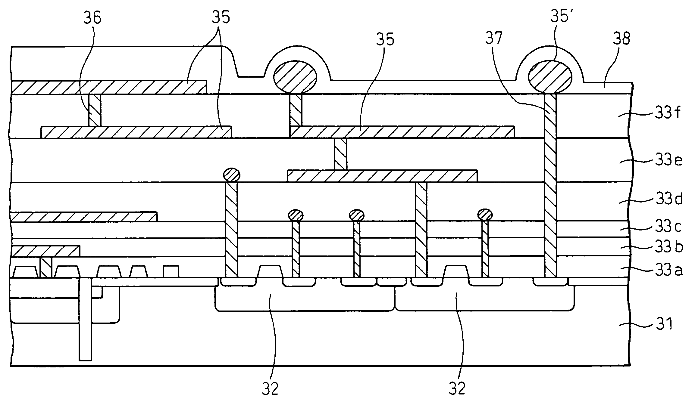
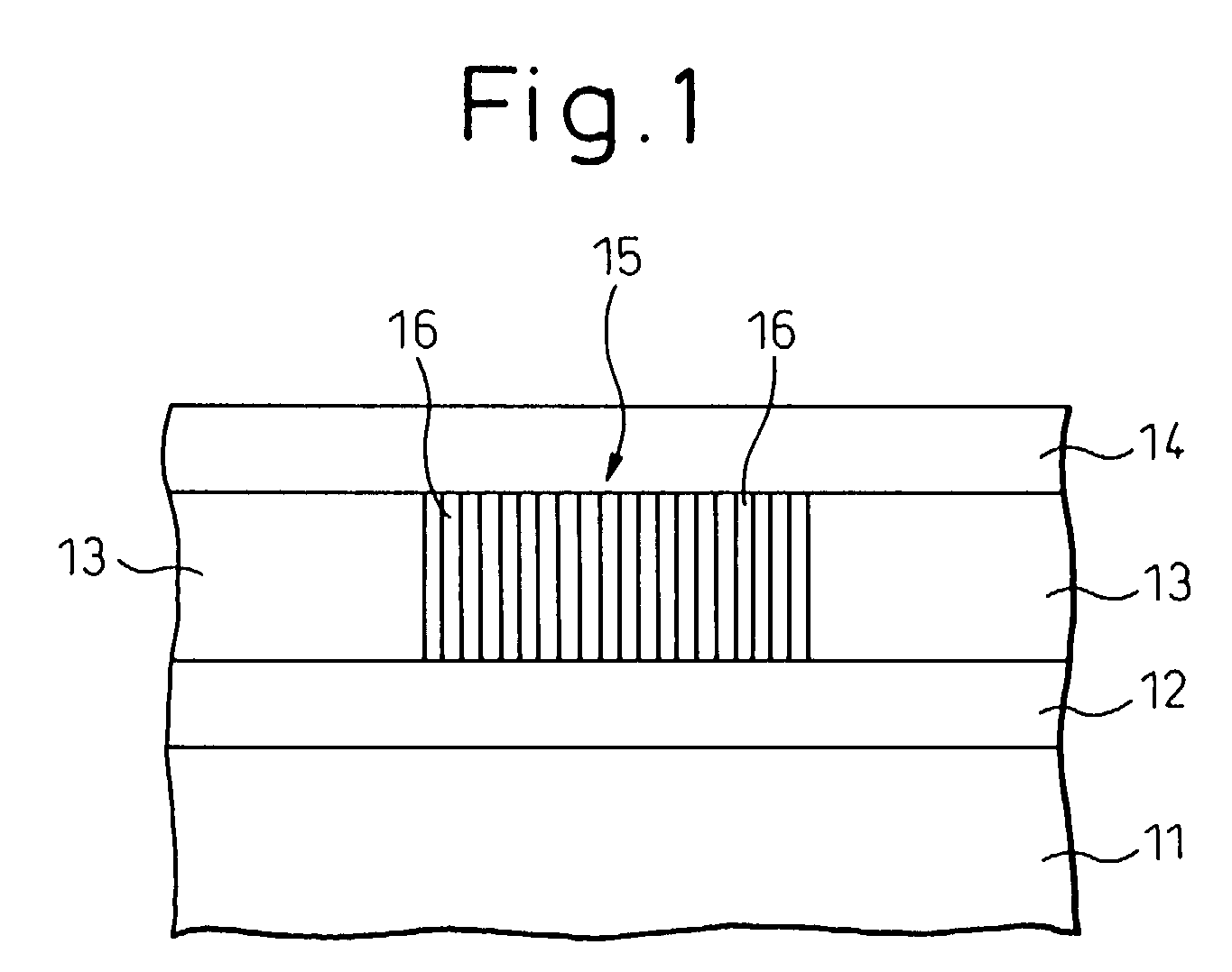
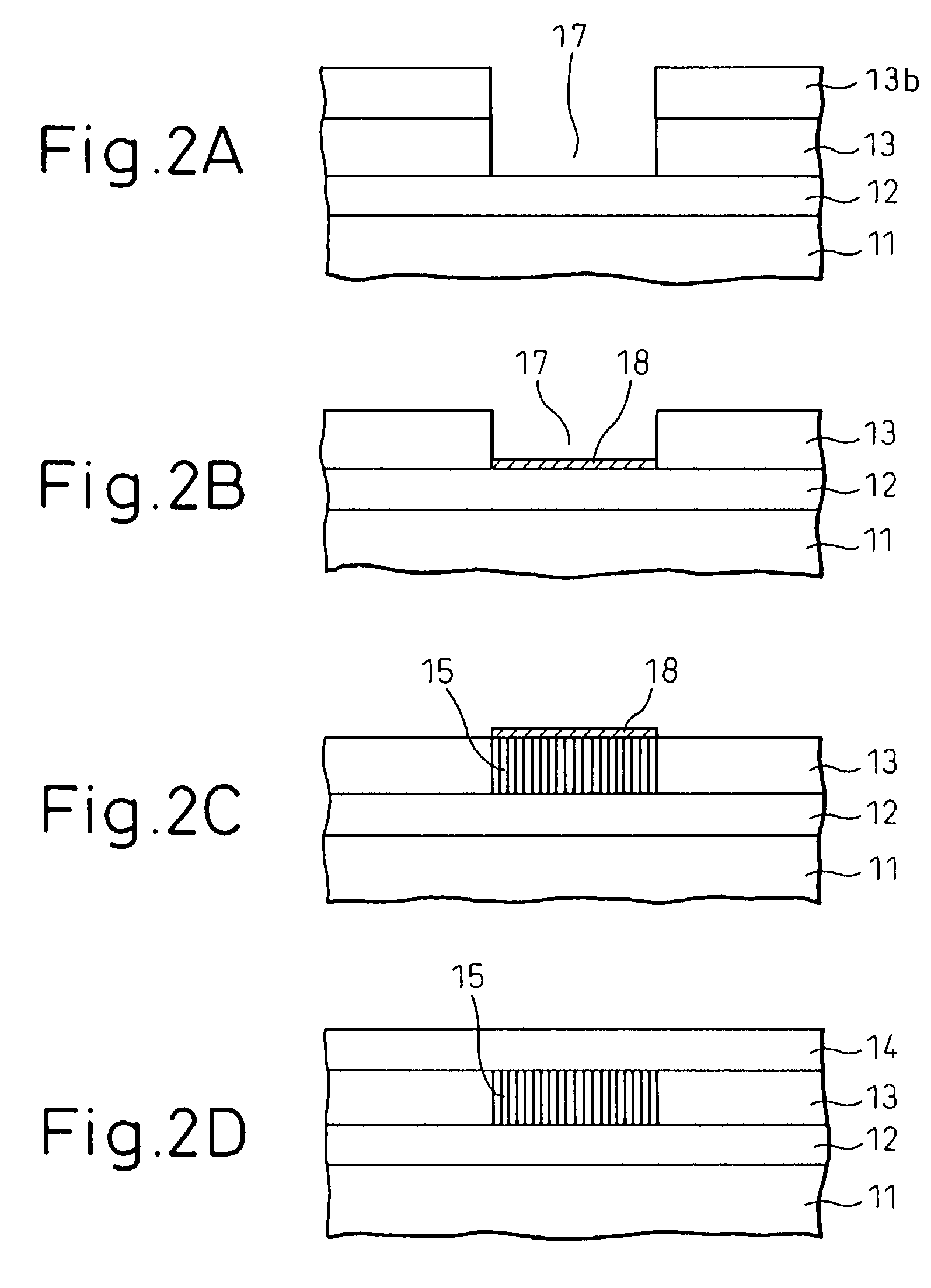
[0071]In the invention, a cylindrical structure made up of carbon atoms, which is a nano-structure based on self-organizing, is used as a material for wiring lines or vias in an integrated circuit device. Such nano-structures include a nano-structure generally known as a carbon nanotube.
[0072]Carbon nanotube is a new carbon-based material, to which attention has recently been paid because of its unique properties. Carbon nanotube has a structure of a cylindrically rolled graphite sheet in which carbon atoms are arranged in the form of united six-membered rings through the strongest bond of sp2, the end of the tube being closed by several six-membered rings accompanied with five-membered rings. Carbon nanotube can have a fined diameter of down to the order of sub-nanometer, with the minimum diameter being 0.4 nanometer. The physical properties of this material are only now being studied, and it is known that the material has a coefficient of thermal conductivity greater than that of ...
PUM
 Abstract
Description
Claims
Application Information