This helps you quickly interpret patents by identifying the three key elements:
Problems solved by technology
Method used
Benefits of technology
Benefits of technology
[0019]As described above, when the high dielectric film made of metal oxide of these types is heated at about 600° C., the crystal defects therein are recovered and thus its insulation properties are improved. However, the film also suffers from grain boundaies by the crystallization of itself and film thickness ununiformity by its phase change. This increases leakage current through the high dielectric film and decreases breakdown voltage of the film.
[0023]If the heat treatment time is set at 0.1 second, the diffusion length L is about 0.3 nm. Since the shortest interatomic distance within a silicon crystal is 0.24 nm, the atoms having moved stay in close proximity to positions at which the atoms had existed before the move. Therefore, the extremely short-time heat treatment enables prevention of the crystallization and phase change in the high dielectric film.
[0026]With the semiconductor device fabrication method of the present invention, the light is irradiated onto the substrate on which the insulating film of high dielectric is formed. If the wavelength of this light is set at a wavelength such that the substrate can absorb the light, an extremely short-time heat treatment of 0.1 second or less can be performed only in the vicinity of the substrate surface. Therefore, when the insulating film of high dielectric is employed as a gate insulating film or a capacitor insulating film, it is possible to prevent leakage current flow resulting from the crystallization or phase change of the insulating film. At the same time, crystal defects in the substrate can be recovered while the growth of an oxide film at the interface of the substrate with the insulating film is suppressed. As a result, a semiconductor device having a small leakage current can be provided while the electrically-equivalent silicon oxide thickness of the film therein is kept small.
[0029]In this case, it is preferable that the inventive fabricating method further comprises, between the first and second steps, the step of selectively introducing dopants into the substrate. This step configuration enables formation of a dopantdiffusion layer which has an extremely shallow junction and a low resistance.
Problems solved by technology
When the gate insulating film, for example, of high dielectric is formed at low temperatures, a number of defects remain in the film.
Method used
Image
Click on the blue label to locate the original text in one second.
Reading with bidirectional positioning of images and text.
Examples
first embodiment
(First Embodiment)
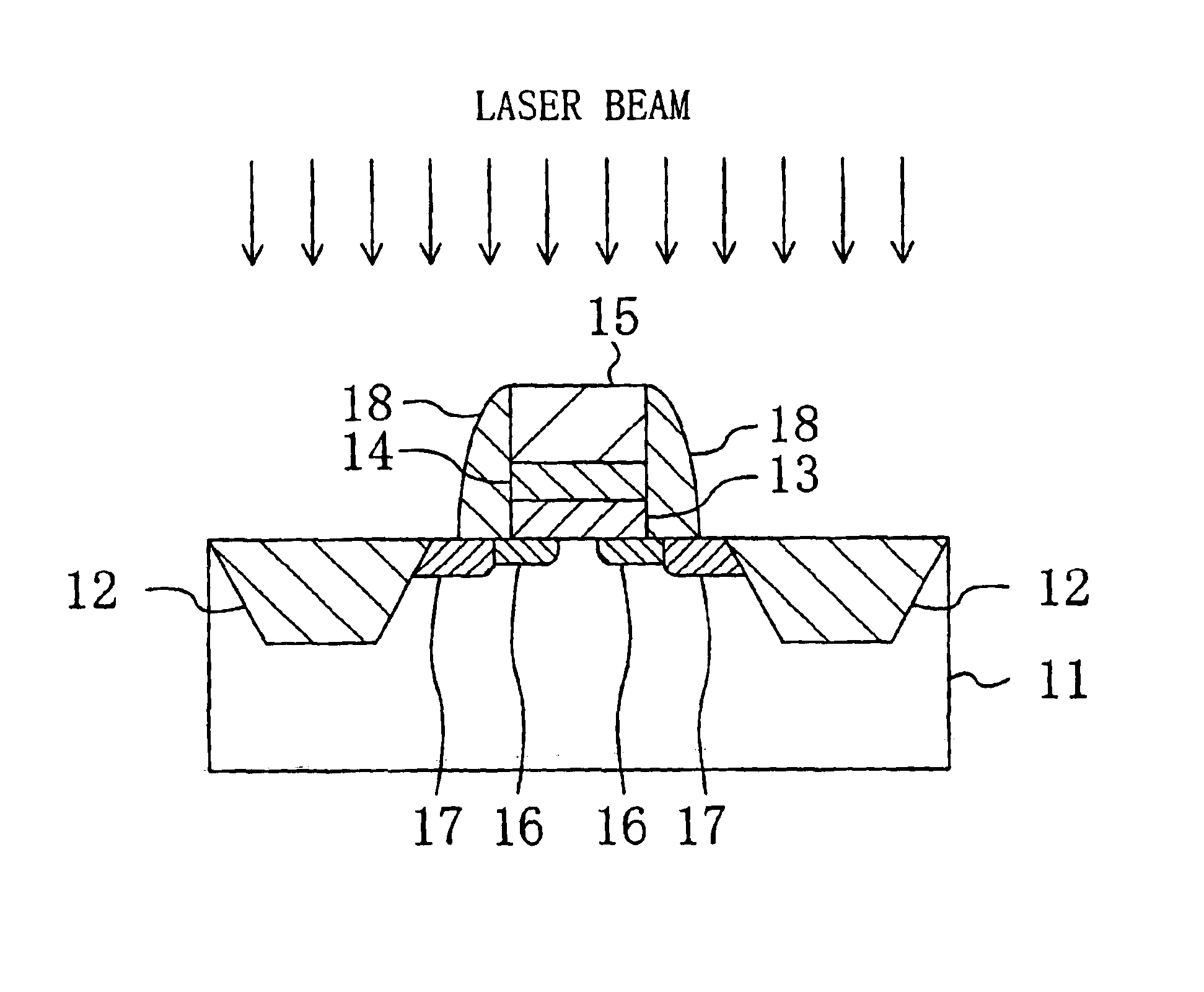
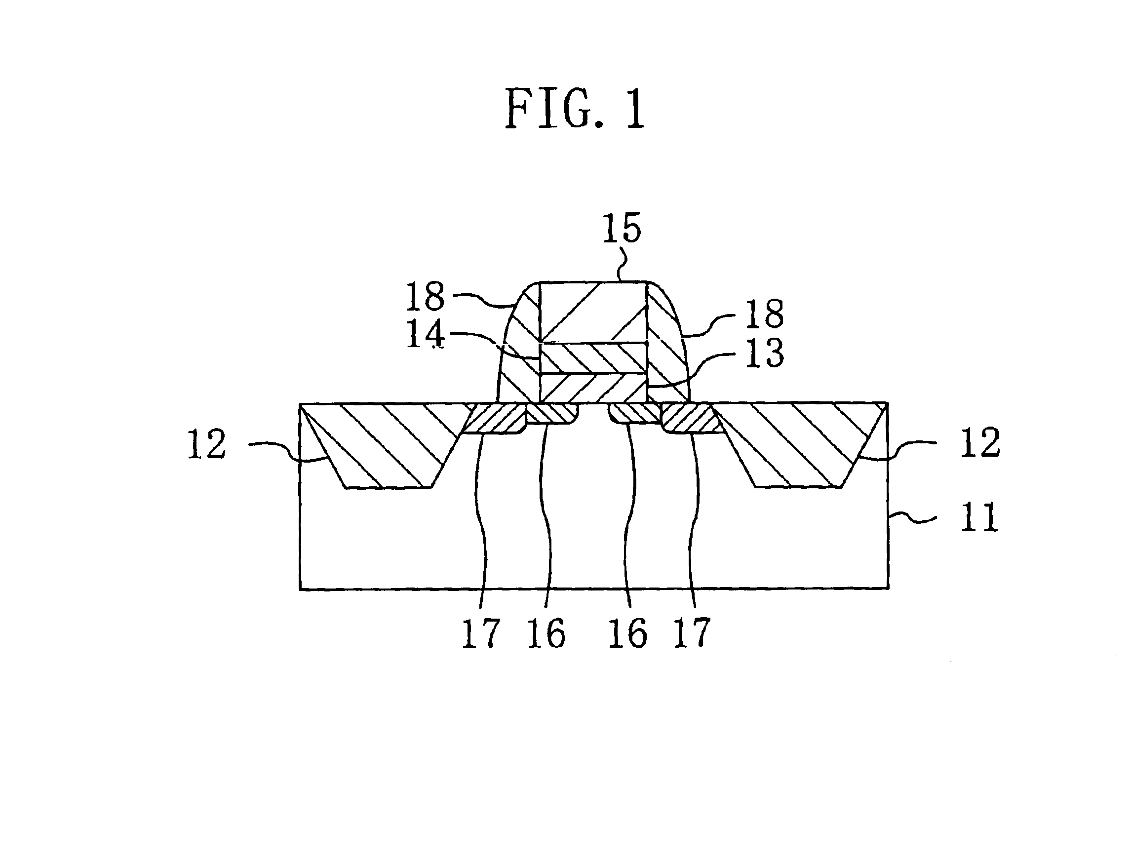
[0045]A first embodiment of the present invention will be described below with reference to the accompanying drawings.
[0046]FIG. 1 is a drawing illustrating a semicoinductor device according to die first embodiment of the present invention and schematically showing a cross-sectional construction of a MIS transistor.
[0047]Referring to FIG. 1, trench isolation regions 12 of silicon oxide (SiO2) are formed in the upper portion of a semiconductor substrate 11 of p-type silicon (Si), for example. The main surface of the semiconductor substrate 11 is defined by the trench isolation regions 12, and the defined region serves as an element formation region.
[0048]An underlying insulting film 13 of silicon oxide having a thickness of about 0.5 nm, a gate insulating film 14 of high dielectric such as hafnium oxide (HfO2) having a thickness of about 4 nm, and a gate electrode 15 of n-type polysilicon are formed, in the listed order, above the element formation region.
[0049]In a...
second embodiment
(Second Embodiment)
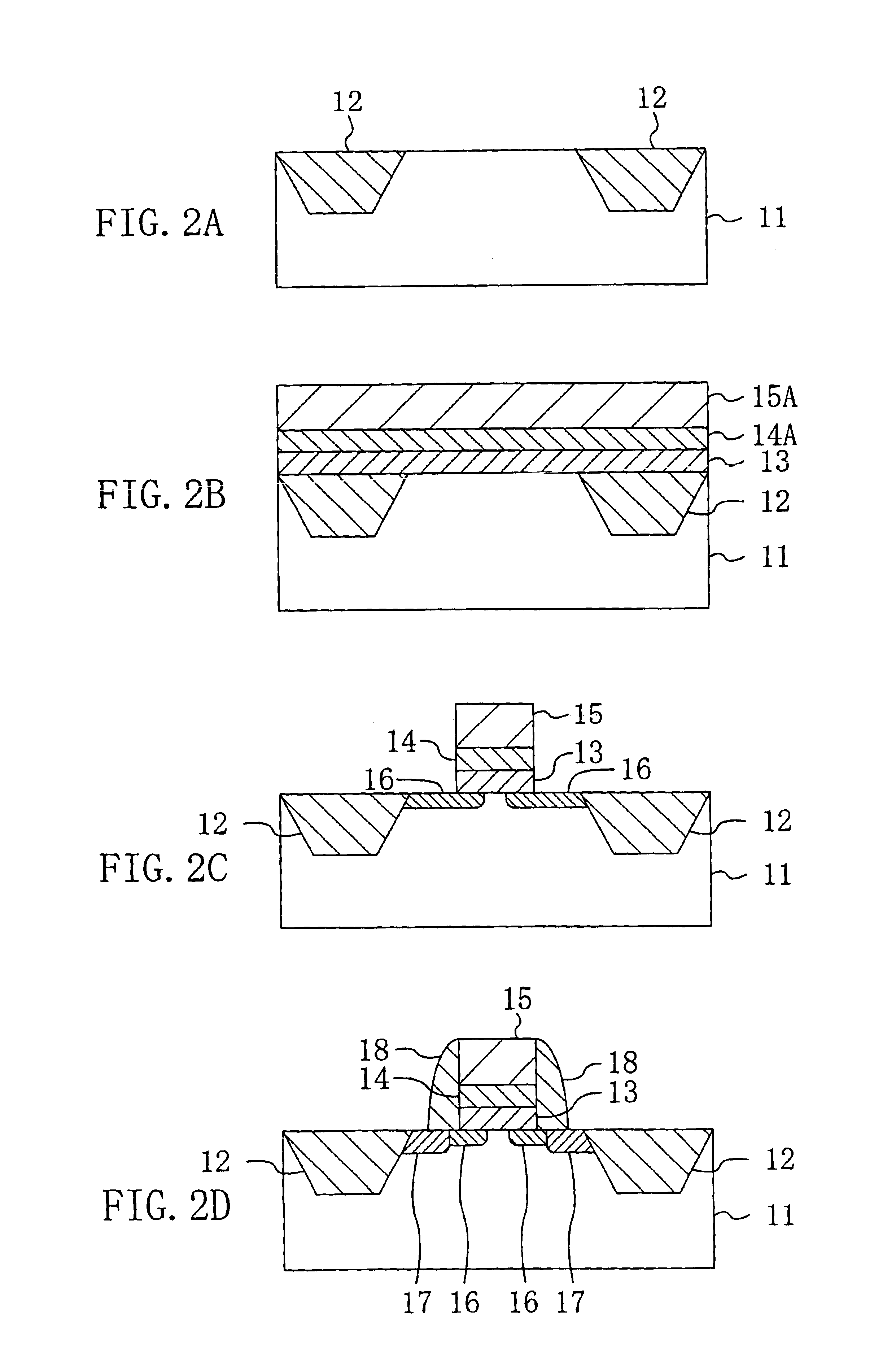
[0068]A second embodiment of the present invention will be described below with reference to the accompanying drawings.
[0069]FIGS. 4A through 4D are sectional views schematically showing process steps of a fabricating method of a semiconductor device according to the second embodiment of the present invention step by step. Also in this description, a semiconductor substrate 11 represents part of a wafer.
[0070]First, as shown in FIG. 4A, trenches are selectively formed by a publicly known technique in the upper portion of the semiconductor substrate 11 of p-type silicon. The formed trenches are filled with silicon oxide to form trench isolation regions 12.
[0071]Subsequently, as shown in FIG. 4B, an underlying insulating film 13 of silicon oxide having a thickness of 0.4 nm is formed by thermal oxidation on the entire surface of the semiconductor substrate 11 including the surfaces of the trench isolation regions 12. On the formed underlying insulating film 13, a hi...
third embodiment
(Third Embodiment)
[0077]A third embodiment of the present invention will be described below with reference to the accompanying drawings.
[0078]FIGS. 5A through 5C are sectional views schematically showing process steps of a fabricating method of a semiconductor device according to the third embodiment of the present invention step by step. The semiconductor device of the third embodiment is a capacitor in a DRAM. Also in this description, a semiconductor substrate 11 represents part of a wafer.
[0079]First, as shown in FIG. 5A, trenches are selectively formed by a publicly known technique in the upper portion of the semiconductor substrate 11 of p-type silicon. The formed trenches are filled with silicon oxide to form trench isolation regions 12. Next, into a region of the semiconductor substrate 11 in which a lower electrode of a capacitor is to be formed, arsenic ions are implanted at an acceleration voltage of about 30 keV and a dose of about 3×10¹⁵ / cm2. Using RTA equipment, heat t...
PUM
Abstract
An underlying insulting film of siliconoxide, a gate insulating film of hafniumoxide, a gate electrode of polysilicon, and side walls of siliconoxide are formed above an element formation region of a semiconductor substrate. In the upper portion of the element formation region of the semiconductor substrate, source and drain areas and extension areas are formed by implantations of respective types. Thereafter, the scan speed of the semiconductor substrate and the pulse interval and the peak power of laser beam are adjusted to irradiate only the vicinity of the surface of the semiconductor substrate with laser beam for 0.1 second so that the vicinity of the surface of the semiconductor substrate has a temperature of 1150 to 1250° C. Thus, heat treatments for the gate insulating film and the source and drain areas are performed.
Description
BACKGROUND OF THE INVENTION[0001]The present invention relates to methods for fabricating a semiconductor device having an insulating film of high dielectric such as hafnium oxide (HfO2) or zirconium oxide (ZrO2).[0002]In recent years, further miniaturization of a MIS transistor has reduced the thickness of a gate insulating film provided in the transistor, which has offered the transistor with high driving power. The thinned gate insulating film, however, causes a direct tunnel current flow between a gate and a channel and an increase in the direct tunnel current boosts the power consumption of the transistor.[0003]Generally, a fine MOS integrated circuit having a gate length of 0.10 μm or smaller requires a very thin gate insulating film whose equivalent silicon oxide thickness Eot is 2 nm or smaller. The equivalent silicon oxide thickness refers to the thickness of an insulating film necessary for having capacitance equivalent to that of a silicon oxide film. In the case where si...
Claims
Application Information
Patent Timeline
Application Date:The date an application was filed.
Publication Date:The date a patent or application was officially published.
First Publication Date:The earliest publication date of a patent with the same application number.
Issue Date:Publication date of the patent grant document.
PCT Entry Date:The Entry date of PCT National Phase.
Estimated Expiry Date:The statutory expiry date of a patent right according to the Patent Law, and it is the longest term of protection that the patent right can achieve without the termination of the patent right due to other reasons(Term extension factor has been taken into account ).
Invalid Date:Actual expiry date is based on effective date or publication date of legal transaction data of invalid patent.

