Programmable logic devices with skewed clocking signals

Inactive Publication Date: 2006-09-12
ALTERA CORP
View PDF12 Cites 42 Cited by
  • Summary
  • Abstract
  • Description
  • Claims
  • Application Information

AI Technical Summary

Benefits of technology

[0011]In accordance with the present invention, programmable logic device architectures are enhanced by providing programmable phase-shifting circuitry to ge

Problems solved by technology

The number of device elements in modern-day PLDs can be very large.
For typical PLDs, most of the data signal propagation delay is due to interconnection delays.
However, the optimization of PLD circuit designs with a large number of device elements and interconnections, is a non-trivial task.
Estimation of the signal propagation delays across a PLD circuit network may require time-consuming or otherwise expensive computations, and usually can be obtained only afte

Method used


Image

  • Programmable logic devices with skewed clocking signals
  • Programmable logic devices with skewed clocking signals
  • Programmable logic devices with skewed clocking signals

Examples


Example

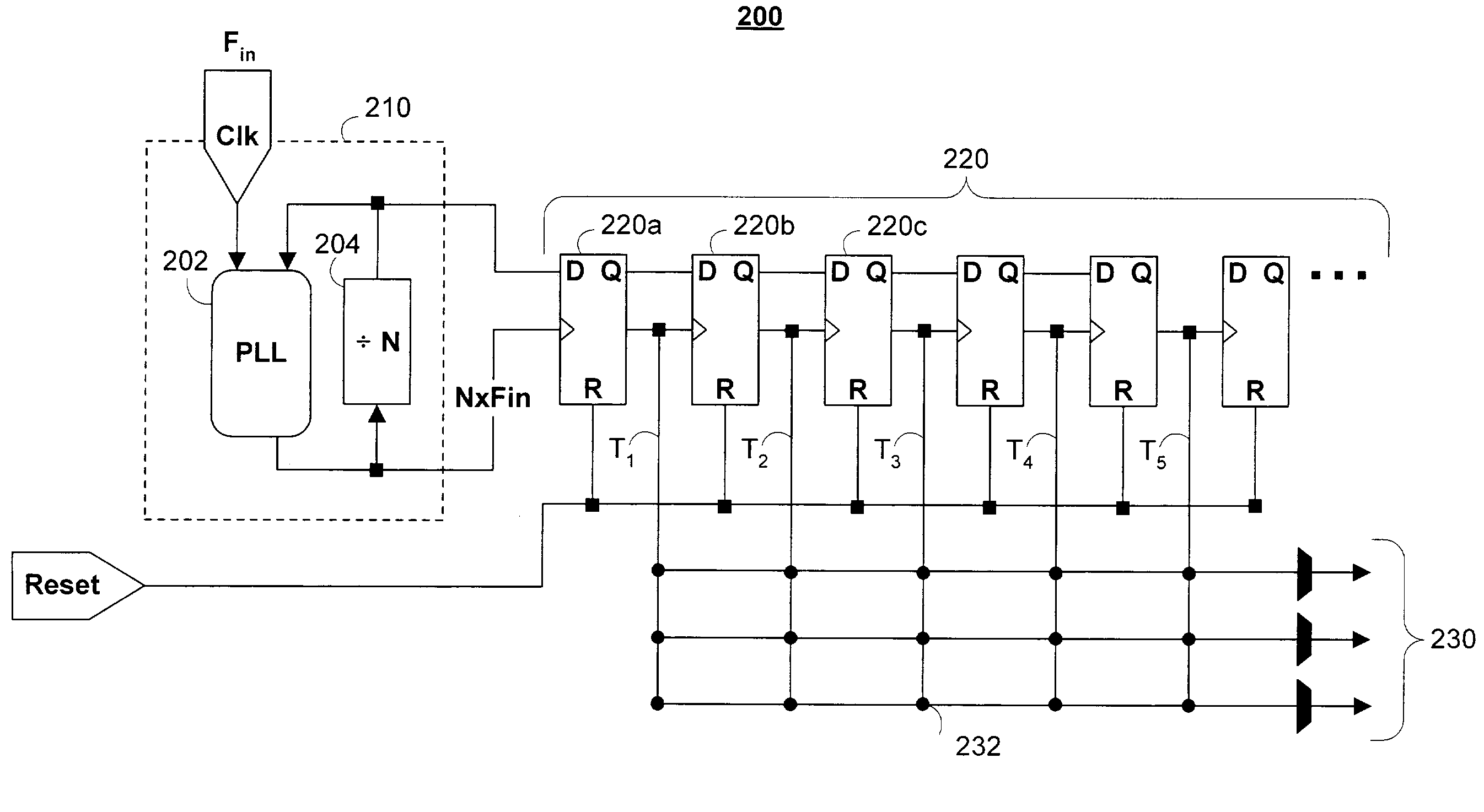
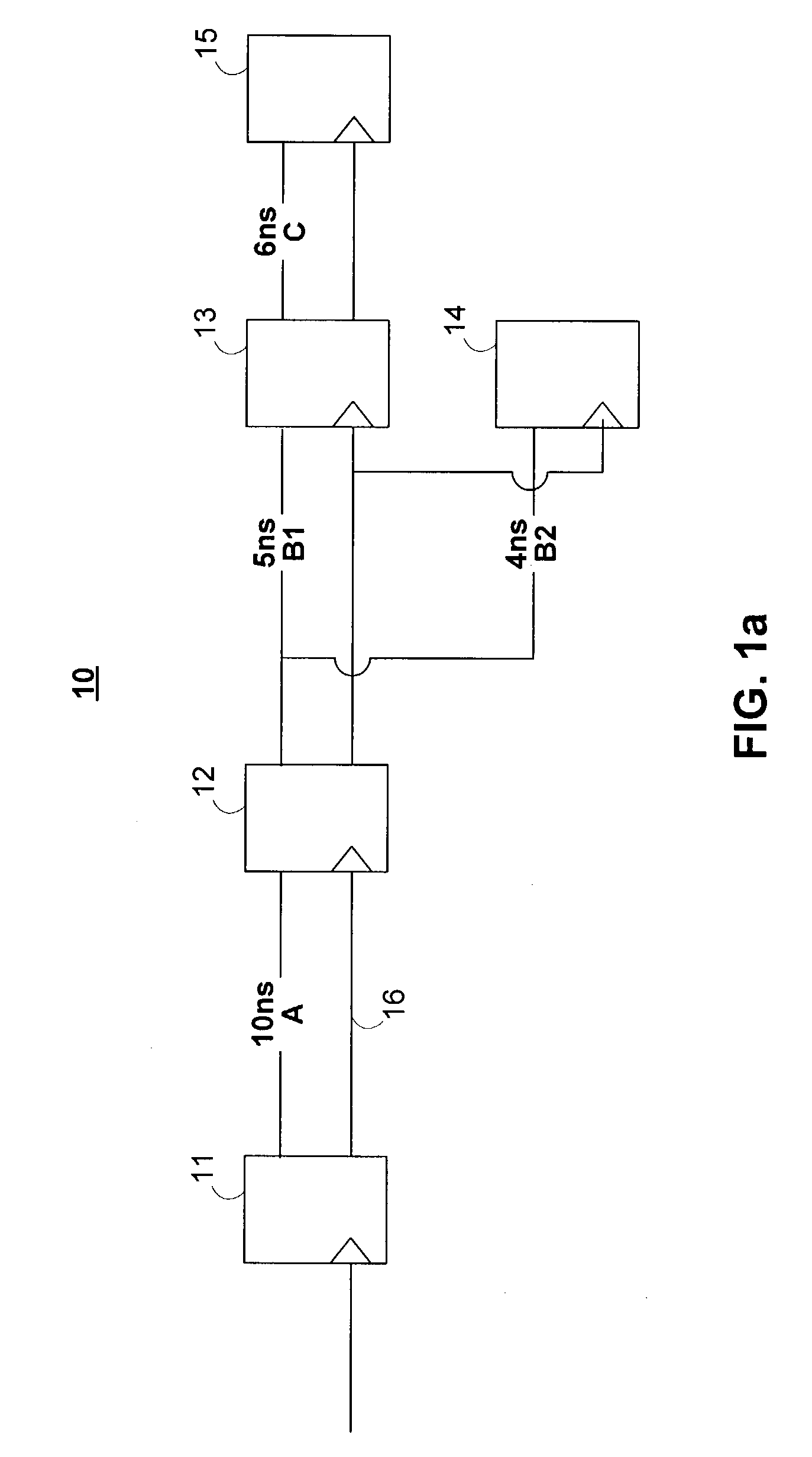
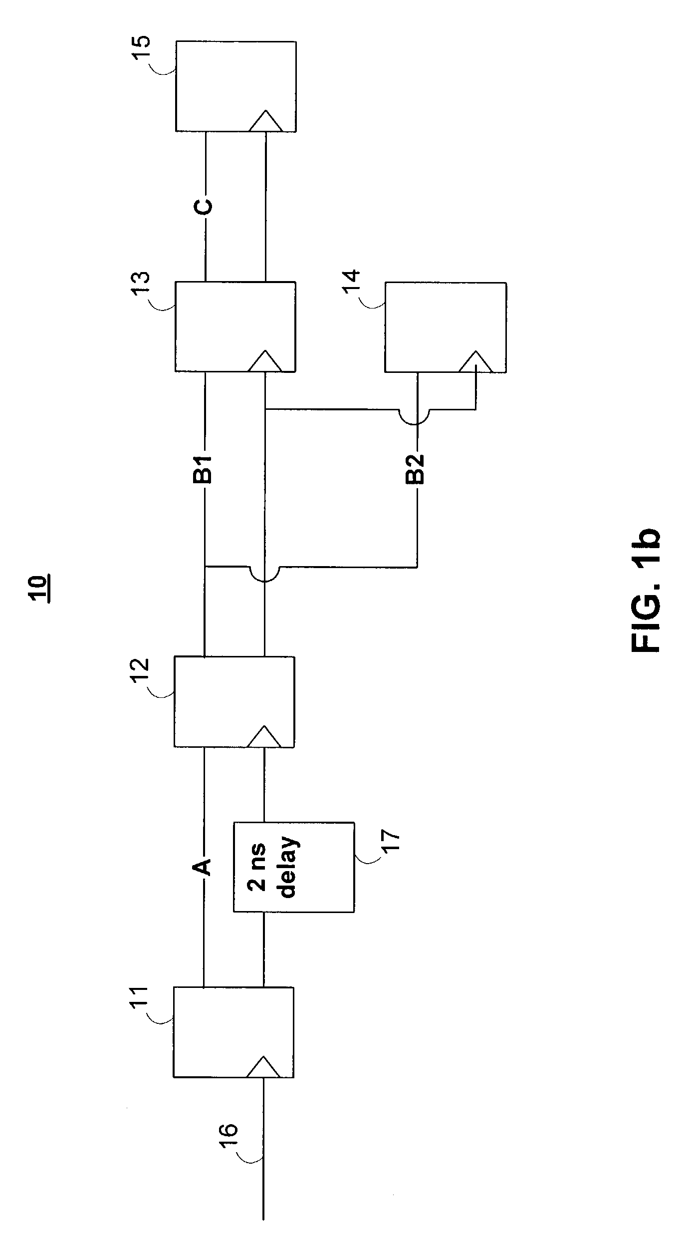
[0027]The concept of clock skew insertion in PLD circuits to improve circuit frequency performance may be understood by reference to an illustrative circuit 10 portion shown in FIGS. 1a and 1b. Circuit 10 portion includes a chain of interconnected registers. FIG. 1a shows, for example, interconnected registers 11, 12, 13, 14 and 15, which are clocked by a clock signal propagating on clock line 16. Data signals are transmitted from register 11 to register 12 over data path A, from registers 12 to registers 13 and 14 over data paths B1 and B2, respectively, and from register 13 to register 15 over data path C. The path lengths (delays) A, B1, B2, and C, may, for example, be about 10 ns, 5 ns, 4 ns, and 6 ns, respectively. Circuit 10 has a maximum operating frequency Fmax (which is inversely related to the longest data path, A=10 ns) of about 100 MHz. FIG. 1b shows modified circuit 10 in which delay circuit 17 inserts a 2 ns delay in the clock signal to register 12 clock input. This in...


PUM


Abstract

A programmable logic device has programmable phase-shifting circuitry. The phase-shifting circuitry is used to generate a set of skewed clock signals that is used to adjust the relative timing of device elements in a circuit synthesized in the programmable logic device. By suitably adjusting the relative timing of the device elements, the circuit critical path lengths are effectively reduced leading to improved circuit frequency performance. Algorithms are provided for establishing clock skew values that lead to improved circuit performance. The algorithms are incorporated in computer aided design tools to enable automatic optimization of circuit designs.

Description

BACKGROUND OF THE INVENTION[0001]Programmable logic devices (PLDs) (or field programmable gate arrays (FPGAs)), are integrated circuit devices with configurable logic networks linked together by programmable interconnection resources. The configurable logic networks may include device elements such as logic cells (e.g., look-up tables (LUTs) or product term logic), memory cells, and input-output cells. Registers (e.g., D-type flip-flops) may be associated with one or more of the device elements. The registers hold and transfer data signals (i.e., variables) between the device elements during PLD operation.[0002]The number of device elements in modern-day PLDs can be very large. These device elements are often architecturally organized into blocks of programmable logic (e.g., gate array or logic array block (“LAB”)), blocks of input-output cells, and blocks of memory (e.g., random access memory (“RAM”)), etc. Groups of these blocks may make up larger blocks (e.g., “MEGALABs”) that ar...

Claims


Application Information

Patent Timeline
IPC IPC(8): G03F7/38
CPCG06F17/5054H03K19/1774H03K5/15066H03K2005/00286G06F30/34
Inventor SINGH, DESHANANDHALL, ANDREW
Owner ALTERA CORP
Why Eureka
Try Eureka