

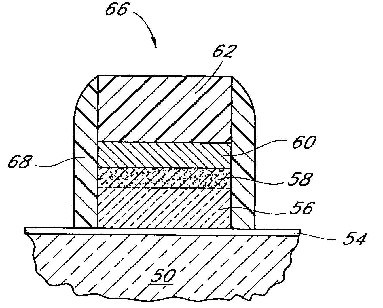
Systems and methods for forming zirconium and/or hafnium-containing layers
a technology of systems and methods, applied in the direction of coatings, metallic material coating processes, chemical vapor deposition coatings, etc., can solve the problems of forming an undesirable siosub>2 /sub>interfacial layer, the traditional use of integrated circuit technology is approaching its performance limits, and the layer no longer effectively functions as an insulator
- Summary
- Abstract
- Description
- Claims
- Application Information
AI Technical Summary
Benefits of technology
Problems solved by technology
Method used
Image

Examples
example 1
Synthesis of Tetraisopropoxysilane, Si[OCH(CH3)2]4
[0068]A dry argon-purged flask equipped with stirrer and thermometer was charged with 100 mL of anhydrous isopropyl alcohol (having a water content of 230 ppm as determined by Karl Fischer Analysis). Then 25 mL of silicon tetrachloride (available from Sigma-Aldrich Co., Milwaukee, Wis.) was added slowly to the alcohol at ambient temperature over a 25 minute period by syringe. During the reaction the contents of the flask formed an emulsion and exothermed to 35° C.
[0069]After standing at ambient conditions for 24 hours, the contents of the flask had formed two layers. The lower layer along with some of the upper layer were transferred to a flask connected to a one-piece distillation apparatus. The isopropyl alcohol was removed from the reaction mixture by distilling at 78° C. and atmospheric pressure using an argon purge. During the distillation, by-product hydrogen chloride gas was vented from the system. Following alcohol and HCl r...
example 2
Atomic Layer Deposition of (Hf,Si)O2
[0070]Using an ALD process, precursor compounds hafnium dimethylamide, Hf(N(CH3)2])4 (Strem Chemicals, Newbury Port, Mass.), and tetraisopropoxysilane, Si[OCH(CH3)2]4, were alternately pulsed for 200 cycles into a deposition chamber containing a silicon substrate with a top layer composed of 1500 Angstroms of p-doped polysilicon. A 350 Å layer of (Hf,Si)O2 was deposited, containing 25 atom % Hf, 10 atom % Si and oxygen. X-ray diffraction analysis (XRD) showed the layer to be amorphous, as measured immediately after the ALD process was completed and also after a 750° C. / 1 minute anneal in oxygen.
PUM
| Property | Measurement | Unit |
|---|---|---|
| temperature | aaaaa | aaaaa |
| pressure | aaaaa | aaaaa |
| temperature | aaaaa | aaaaa |
Abstract
Description
Claims
Application Information