Single crystal GaN substrate semiconductor device

a gallium nitride and single crystal technology, applied in the direction of semiconductor lasers, crystal growth process, polycrystalline material growth, etc., can solve the problems of inability to make a gallium nitride melt, inability to obtain wide, high-quality gan single crystal wafers, and inability to make a gan single crystal melt, etc., to reduce the density of regions and reduce the effect of foggy dislocations

Active Publication Date: 2006-09-26
SUMITOMO ELECTRIC IND LTD
View PDF7 Cites 28 Cited by
  • Summary
  • Abstract
  • Description
  • Claims
  • Application Information

AI Technical Summary

Benefits of technology

[0124]The present invention solves the problem of uncertainty of the pit positions which would allow LD active stripes to overlap pits by predetermining the pit positions by regular, periodic seed implantation. Programmable pit positions are an advantage of the present invention.
[0125]The principles founding the present invention have been described.SUMMARY OF THE INVENTION
[0126]This invention makes the best use of seeds made on a substrate and facet growth following the seeds. The facet growth minimizes dislocation density of regions except closed defect accumulating regions (H) by sweeping many dislocations into the bottoms of facet pits and the closed defect accumulating regions (H) hold many dislocations captive. The seed-defined closed defect accumulating regions (H) and the facet growth enable us to accomplish all the aforementioned three purposes,
[0127](1) a decrease of foggy dislocations leaking from the centers of the facet pits,
[0128](2) an elimination of planar defect assemblies at the centers of the facet pits, and
[0129](3) a control of the positions of the defect assemblies at the centers of the facet pits.

Problems solved by technology

But, immaturity of crystal growth technology forbids device makers from obtaining wide, high quality GaN single crystal wafers till now.
However, it is impossible to make a melt of gallium nitride (GaN), since heating does not convert GaN polycrystals into a melt but sublimes GaN polycrystals into vapor.
Thus, Czochralski method and Bridgman method which a melt polycrystal material into a melt, cool a part of the melt and make a large single crystal bulk solid at a thermal equilibrium, are unavailable for making a GaN single crystal.
However, a sapphire substrate which is chemically stable and physically rigid cannot be eliminated after the GaN film has been grown on the sapphire substrate.
However, the separation of the sapphire substrates from the GaN films is difficult even by high power lasers.
However, it is found that thick GaN is not grown upon a GaAs substrate.
Perhaps differences of lattice constants and thermal expansions between GaAs and GaN cause the difficulty of growing thick GaN on the GaAs substrate.
However, when the GaN substrate is of low quality, no good devices can be produced on the GaN substrate.
Reduction of dislocations is insufficient.
ELO-made GaN crystals are unsatisfactory as a GaN substrate upon which InGaN type LDs are fabricated.
The inventors noticed that the facet growth method has still problems for producing GaN wafers for making LD chips.
Occurrence of the nebular hazy dislocation dispersion was a drawback of the previous facet growth.
The occurrence of the hazy dislocation nebulae is the first problem of the previous facet growth.
The second problem is planar defect assemblies which are born by gathering dislocations to the pit bottoms and inclining to each other at 60 degrees.
In addition to the hazy dislocation nebulae, the radially extending planar defects assemblies are a serious problem for an LD substrate, since the planar defects would induce degeneration and would restrict lifetime of LDs.
Occurrence and distribution of pits are stochastic, accidental and unprogrammable.
The previous facet growth method which reduces dislocations by growing facet pits without burying, has a weak point of undeterminable positions of pits.
It is impossible to previously determine or know the spots at which facet pits happen.
Uncontrollability of pit positions is a serious problem.
Planar defects have large sizes.
Such a method which cannot determine the positions at which dislocation bundles happen is inconvenient.
The occurrence of dislocation bundles is unavoidable.
The use of the metallorganic compound (TMG) may induce contamination by carbon.
Designations of crystal orientations are not well known even to the skilled.
There are confusion, misunderstanding and misuse of crystallographical symbols in many academic reports or patent descriptions.
Poor symmetry deprives sapphire of cleavage.
All the three are difficult problems.
The serious problem of the previous facet growth of the inventors which maintains facets and pits without burying the facets was an unstable state of defect assemblies at pit bottoms.
Occurrence of pits and positions of pits were uncontrollable.
One problem is the dislocation-assembled state at the pit bottoms.
The tendency incurs difficult problems.
This is the aforementioned problem (1) of the hazy dislocation dispersion.
When a plurality of facet pits merge into a big pit, the number of the dislocations which converge to the pit center is also increased and large planar defect assemblies are produced.
The relaxed hazy dislocation bundles is an obstacle of making devices on the GaN substrate which has been made by the previous method.
An increase of the area of hazy dislocation bundles lowers the quality of devices and decreases the yield of making devices.
A serious problem of the previous contrivance is that the dislocations once gathered to the centers of the facet pits are not permanently captured but are soon released from the bottoms of the facet pits (relaxing bundles 15 in FIG.
The next problem is how to make a grain boundary K encapsulating the closed defect accumulating region (H).

Method used


Image

  • Single crystal GaN substrate semiconductor device
  • Single crystal GaN substrate semiconductor device
  • Single crystal GaN substrate semiconductor device

Examples


embodiment 3 (

Kinds of Masks)

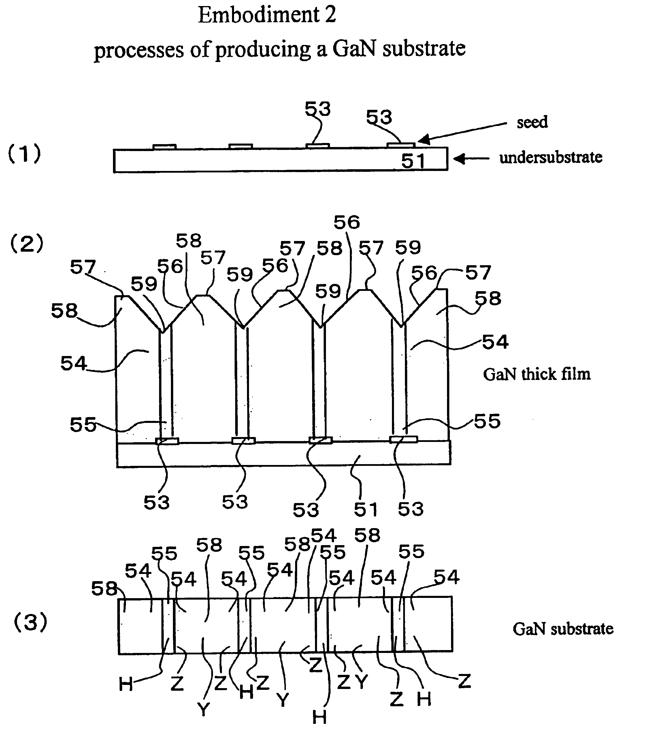
[0456]A plurality of GaAs wafers having a (111) As surface are prepared as undersubstrates for examining the dislocation dependence upon materials of the mask. Different masks are made by coating the (111) As GaAs wafers with different materials.

[0457](I) A 0.15 mu.m thick Si.sub.3N.sub.4 (silicon nitride) film is directly formed on the (111) GaAs wafer.

[0458](J) A 0.2 .mu.m thick Pt (platinum) film is directly formed on the (111) GaAs wafer.

[0459](K) A 0.2 .mu.m thick W (tungsten) film is directly formed on the (111) GaAs wafer.

[0460](L) A 0.1 .mu.m thick SiO.sub.2 (silicon dioxide) film is directly formed on the (111) GaAs wafer.

[0461](M) A 0.1 .mu.m thick SiO.sub.2 (silicon dioxide) film is directly formed on the (111) GaAs wafer.

[0462]Seed patterns are tailored by painting a resist on the film-coated GaAs wafers I.about.M and etching parts of the films from the film / GaAs selectively by photolithography. The SiN film (I), the Pt film (J) and the W film (K) are allo...


PUM

PropertyMeasurementUnit
diameteraaaaaaaaaa
thicknessaaaaaaaaaa
thickaaaaaaaaaa

Abstract

Seeds are implanted in a regular pattern upon an undersubstrate. A GaN crystal is grown on the seed implanted undersubstrate by a facet growth method. The facet growth makes facet pits above the seeds. The facets assemble dislocations to the pit bottoms from neighboring regions and make closed defect accumulating regions (H) under the facet bottoms. The closed defect accumulating regions (H) arrest dislocations permanently. Release of dislocations, radial planar defect assemblies and linear defect assemblies are forbidden. The surrounding accompanying low dislocation single crystal regions (Z) and extra low dislocation single crystal regions (Y) are low dislocation density single crystals.

Description

[0001]This Application is a divisional of application Ser. No. 10 / 246,559 filed on Sep. 19, 2002 now U.S. Pat. No. 6,667,184BACKGROUND OF THE INVENTION[0002]1. Field of the Invention[0003]This invention relates to a single crystal gallium nitride (GaN) substrate for producing blue light emitting diodes (LEDs) and blue light laser diodes (LDs) composed of group 3-5 nitride type semiconductors, a method of growing a single crystal gallium nitride substrate, and a method of producing a single crystal gallium nitride substrate.[0004]This application claims the priority of Japanese Patent Applications No.2001-284323 filed on Sep. 19, 2001 and No.2002-230925 filed on Aug. 8, 2002, which are incorporated herein by reference.[0005]Blue light emitting diodes (LEDs) based upon the group 3-5 nitride type semiconductors (InGaN, GaN) have been manufactured, sold and used on a large scale. Almost all the practical nitride type LEDs are made upon insulating sapphire (.alpha.−Al.sub.2O.sub.3) subst...

Claims


Application Information

Patent Timeline
Patent Type & Authority Patents(United States)
IPC IPC(8): H01L33/00C30B29/38C30B25/02C30B25/18H01L21/20H01L21/205H01L33/32H01S5/323
CPCC30B25/02C30B25/18C30B25/183C30B29/406H01L21/02381H01L21/02395H01L21/02647H01L21/02433H01L21/02458H01L21/0254H01L21/02609H01L21/02642H01L21/0242H01L21/20
Inventor MOTOKI, KENSAKUOKAHISA, TAKUJINAKAHATA, SEIJIHIROTA, RYUUEMATSU, KOJI
Owner SUMITOMO ELECTRIC IND LTD
Why Eureka
Try Eureka