
Systems and methods for forming strontium- and/or barium-containing layers

a technology of strontium and barium, applied in the direction of polycrystalline material growth, crystal growth process, chemically reactive gas, etc., can solve the problems of reducing the conformality of the layer, and reducing the efficiency of the layer. , to achieve the effect of minimizing the detrimental gas phase reaction and improving the control of the thickness of the layer

Inactive Publication Date: 2006-10-03
MICRON TECH INC
View PDF15 Cites 125 Cited by
  • Summary
  • Abstract
  • Description
  • Claims
  • Application Information

AI Technical Summary

Benefits of technology

[0026]“Atomic layer deposition” (ALD) as used herein refers to a vapor deposition process in which numerous consecutive deposition cycles are conducted in a deposition chamber. Typically, during each cycle the metal precursor is chemisorbed to the substrate surface; excess precursor is purged out; a subsequent precursor and / or reaction gas is introduced to react with the chemisorbed layer; and excess reaction gas (if used) and by-products are removed. As compared to the one cycle chemical vapor deposition (CVD) process, the longer duration multi-cycle ALD process allows for improved control of layer thickness by self-limiting layer growth and minimizing detrimental gas phase reactions by separation of the reaction components. The term “atomic layer deposition” as used herein is also meant to include the related terms “atomic layer epitaxy” (ALE) (see U.S. Pat. No. 5,256,244 (Ackerman)), molecular beam epitaxy (MBE), gas source MBE, organometallic MBE, and chemical beam epitaxy when performed with alternating pulses of precursor compound(s), reaction gas and purge (i.e., inert carrier) gas.

Problems solved by technology

The continuous shrinkage of microelectronic devices such as capacitors over the years has led to a situation where the materials traditionally used in integrated circuit technology are approaching their performance limits.
However, when the SiO2 layer is thinned to 1 nm (i.e., a thickness of only 4 or 5 molecules), as is desired in the newest microelectronic devices, the layer no longer effectively performs as an insulator due to the tunneling current running through it.
At higher temperatures the precursor compound transformation becomes the limiting factor, causing a degradation of the conformality.

Method used


Image

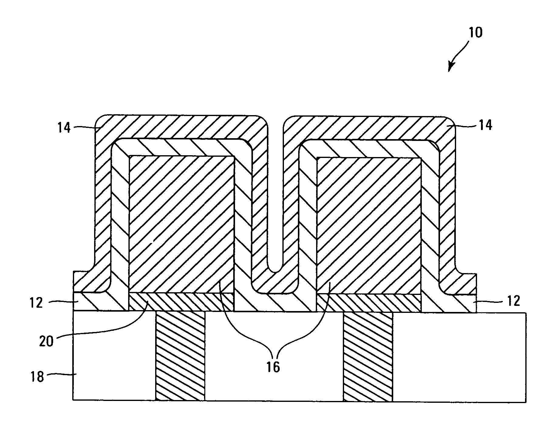
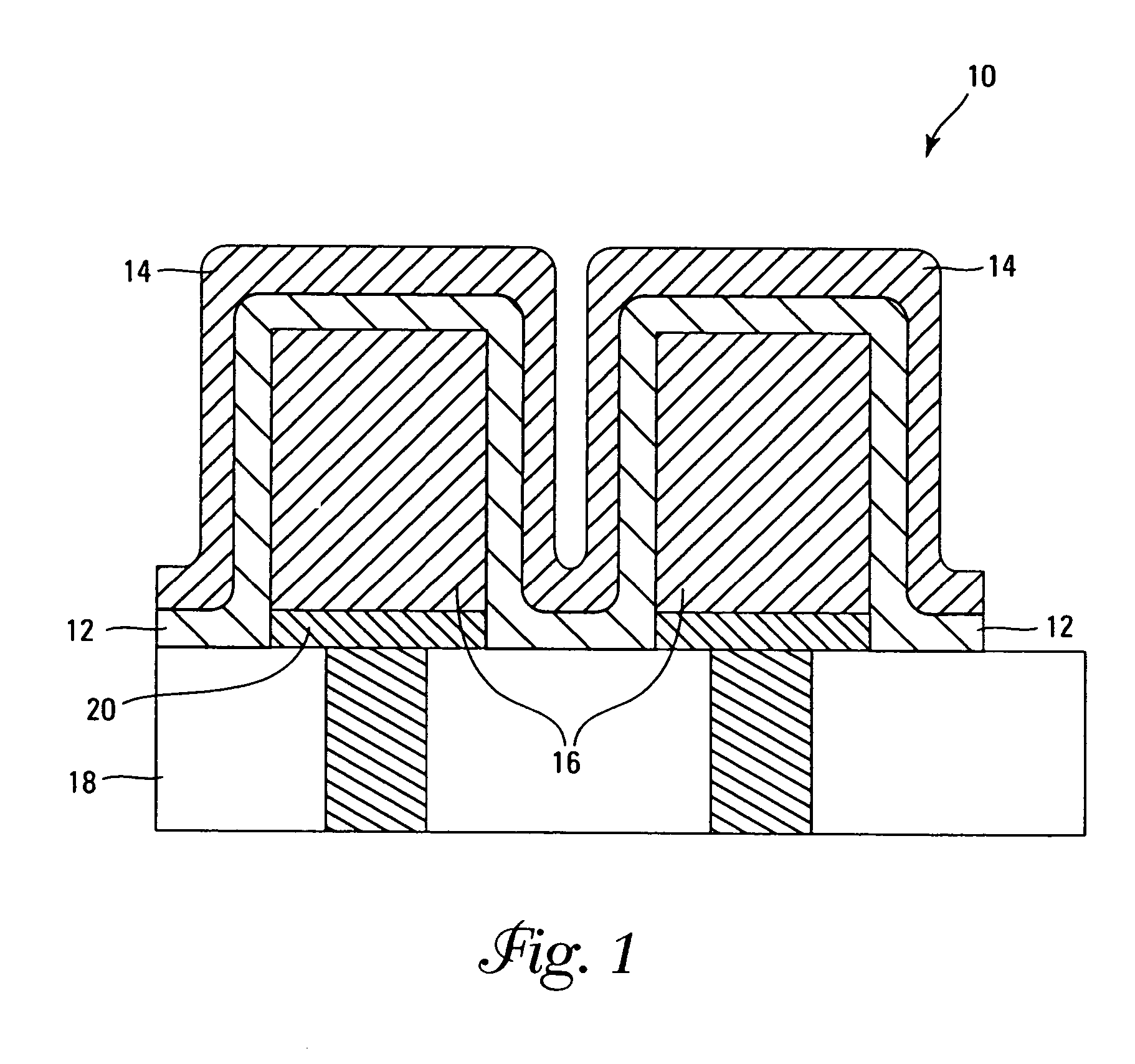
  • Systems and methods for forming strontium- and/or barium-containing layers
  • Systems and methods for forming strontium- and/or barium-containing layers
  • Systems and methods for forming strontium- and/or barium-containing layers

Examples


example 1

Atomic Layer Deposition of SrTiO3

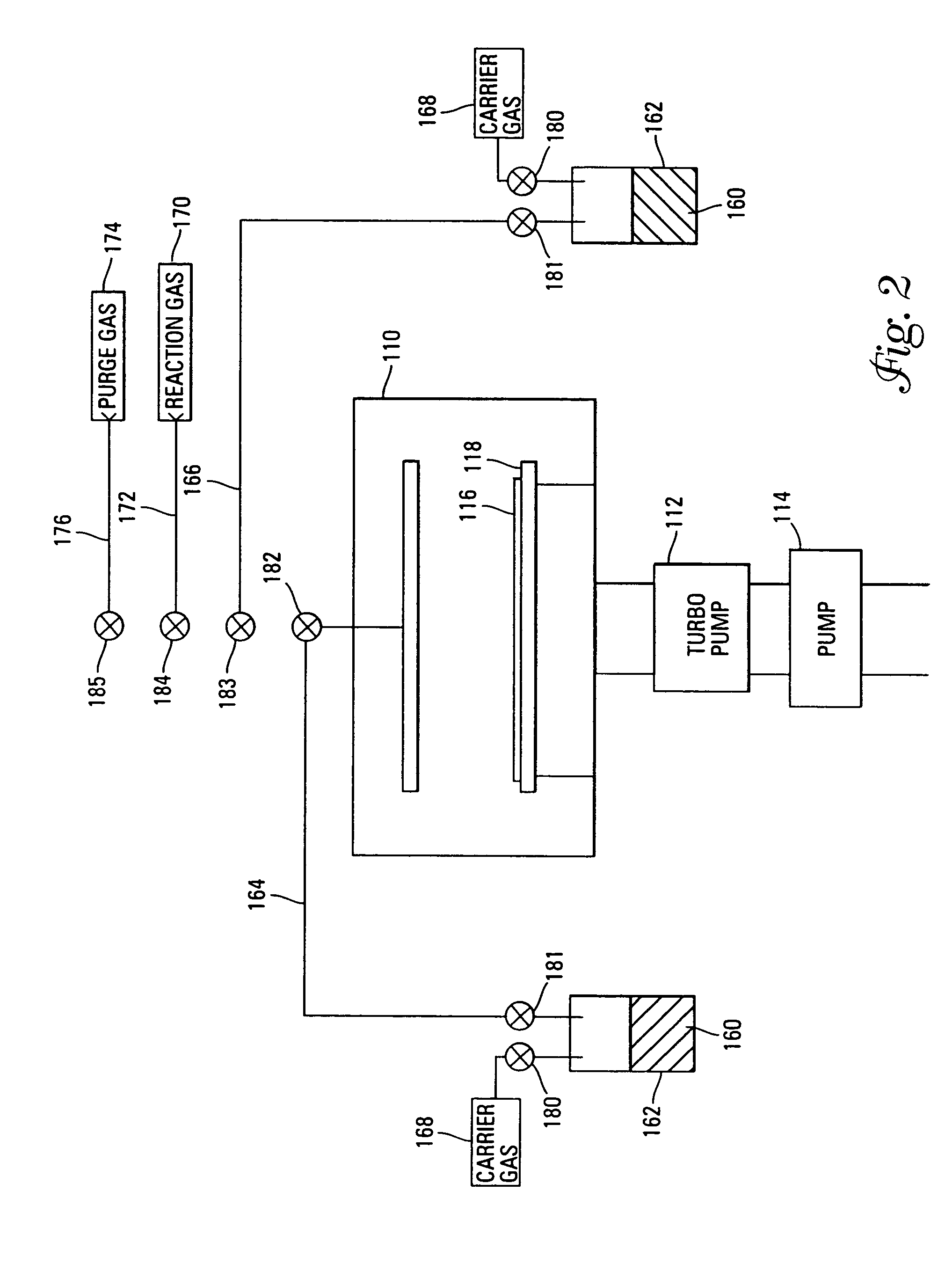
[0062]Separate reservoirs of the compounds Sr[N(SiMe3)2]2 and titanium isopropoxide are attached to a vapor deposition chamber and heated to 130° C. and 45° C., respectively. Lines and valves connecting the reservoirs to the chamber are maintained 20° C. above the reservoir temperature The Sr[N(SiMe3)2]2 remains solid; subliming into the vapor phase. The titanium source is a liquid with reasonable vapor pressure under these conditions. The substrate is a silicon wafer which has been processed up to the bottom electrode of the capacitor. The substrate is on a heated stage held at 300° C. The chamber is pumped down to a base pressure of 10−5 torr before the ALD cycles are initiated and remains under dynamic vacuum for the duration of the deposition. The precursors are pulsed into the chamber using pneumatic actuated valves under computer control. A Sr-source pulse of 1 second is followed by a 1-second purge gas pulse of argon followed by a 3-second pu...

example 2

Atomic Layer Deposition of (Ba,Sr)TiO3

[0063]The deposition is carried out in a fashion similar to that described in Example 1. An additional reservoir of Ba[N(SiMe3)2]2 is connected to the chamber and heated to 160° C. The pulse sequence described above for SrTiO3 is used except that every other pulse of the Sr-source is replaced by a Ba-source pulse. The film can also be made richer in either Sr or Ba by using more pulses of the desired precursor in the total number of pulses.


PUM

PropertyMeasurementUnit
Thicknessaaaaaaaaaa
Dielectric polarization enthalpyaaaaaaaaaa
Semiconductor propertiesaaaaaaaaaa

Abstract

A method of forming (and apparatus for forming) a layer, such as a strontium titanate, barium titanate, or barium-strontium titanate layer, on a substrate by employing a vapor deposition method, particularly a multi-cycle atomic layer deposition process.

Description

[0001]This is a continuation of application Ser. No. 10 / 230,131, filed Aug. 28, 2002, now U.S. Pat. No. 6,730,164, which is incorporated herein by reference.FIELD OF THE INVENTION[0002]This invention relates to methods of forming a layer on a substrate using a vapor deposition process, particularly a multi-cycle atomic layer deposition (ALD) process, using one or more Group IIA metal precursor compounds and optionally other metal (e.g., titanium) precursor compounds, typically in the presence of one or more reaction gases. The precursor compounds and methods are particularly suitable for the formation of strontium and / or barium titanate dielectric layers on semiconductor substrates or substrate assemblies.BACKGROUND OF THE INVENTION[0003]Capacitors are the basic energy storage devices in random access memory devices, such as dynamic random access memory (DRAM) devices and ferroelectric memory (FERAM) devices. They consist of two conductors, such as parallel metal or polysilicon plat...

Claims


Application Information

Patent Timeline
IPC IPC(8): C30B25/02C23C16/40C23C16/44C23C16/455C30B23/00C30B25/00C30B25/04C30B25/14C30B25/16C30B28/12C30B28/14H01L21/00H01L21/02H01L21/316
CPCC23C16/409C23C16/45531H01L21/31691H01L28/55H01L21/02205H01L21/02175H01L21/0228H01L21/02197H01L21/02271
Inventor VAARTSTRA, BRIAN A.UHLENBROCK, STEFAN
Owner MICRON TECH INC
Learn More