Semiconductor device having El layer and sealing material

a technology of sealing material and semiconductor film, which is applied in the direction of discharge tube luminescnet screen, discharge tube/lamp details, electric discharge lamps, etc., can solve the problems of powder explosion, slow speed of reduced pressure cvd film formation, and process that uses plasma cvd has a disadvantage from a workplace safety perspective, so as to promote crystallization and reduce the concentration of catalytic elements

Inactive Publication Date: 2006-10-24
SEMICON ENERGY LAB CO LTD
View PDF30 Cites 59 Cited by
  • Summary
  • Abstract
  • Description
  • Claims
  • Application Information

AI Technical Summary

Benefits of technology

[0014]In accordance with the background described above, an object of the present invention is to provide a process that can deposit a film at low temperature, and by forming an amorphous semiconductor film using sputtering method of superior productivity, and that has a high level of safety.
[0015]In addition, an object of the present invention is to provide a semiconductor device, which includes a semiconductor circuit made from a semiconductor element with high quality electrical characteristics. The high quality electrical characteristics result by using sputtering to form an amorphous semiconductor film and then crystallizing the film, with the resulting crystalline semiconductor film as the active layer forming a good interface with the insulating film.
[0018]This type of composition realizes a TFT with good electrical characteristics through use of a process that provides a safe work environment.
[0032]A third aspect of the manufacturing method of the present invention is a method for manufacturing a semiconductor device which includes a semiconductor circuit made from a semiconductor element, and is characterized by comprising the steps of forming a semiconductor film by sputtering on top of the surface of an insulator, adding catalytic elements into at least a portion of the semiconductor film to promote crystallization, forming a crystalline semiconductor film by crystallizing the semiconductor film, and reducing the concentration of the catalytic elements throughout the crystalline semiconductor film.
[0035]A sixth aspect of the manufacturing method of the present invention is a method for manufacturing a semiconductor device which includes a semiconductor circuit made from a semiconductor element, and is characterized by comprising the steps of adding catalytic elements into at least a portion of the surface of an insulator to promote crystallization, forming a semiconductor film by sputtering, forming an insulating film in contact with the semiconductor film, forming a crystalline semiconductor film by crystallizing the semiconductor film while it is contact with the insulating film, and reducing the concentration of the catalytic elements throughout the crystalline semiconductor film.

Problems solved by technology

The speed that reduced pressure CVD can form an amorphous semiconductor film is slow, a disadvantage from a manufacturing perspective.
This powder is ultrafine, and is known to cause powder explosions when exposed to the atmosphere.
Therefore, due to the great danger of an explosion, a process that uses plasma CVD has a disadvantage from a workplace safety perspective.
This means the surface of the crystallized silicon film, which is to become the active layer, is exposed to the atmosphere and may become either contaminated with impurities (oxygen, moisture, boron, sodium) or oxidized before the gate insulating film can be formed.
Then when the gate insulating film is laminated on top, the active layer, especially the interface between the channel formation region and the gate insulating film, properties drop, and this causes a drop in the electrical characteristics of the TFT.
This is especially true for the atmosphere in clean rooms, in which boron (boric) from the HEPA type filter generally in use can cause boron to intermix with the exposed surface of the film in uneven concentrations.

Method used


Image

  • Semiconductor device having El layer and sealing material
  • Semiconductor device having El layer and sealing material
  • Semiconductor device having El layer and sealing material

Examples


embodiment 1

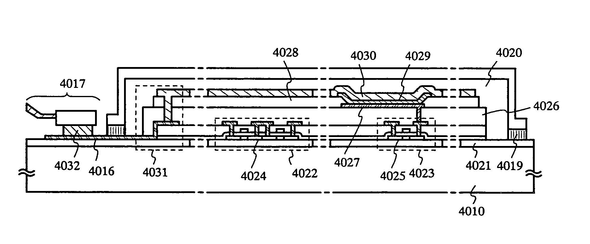
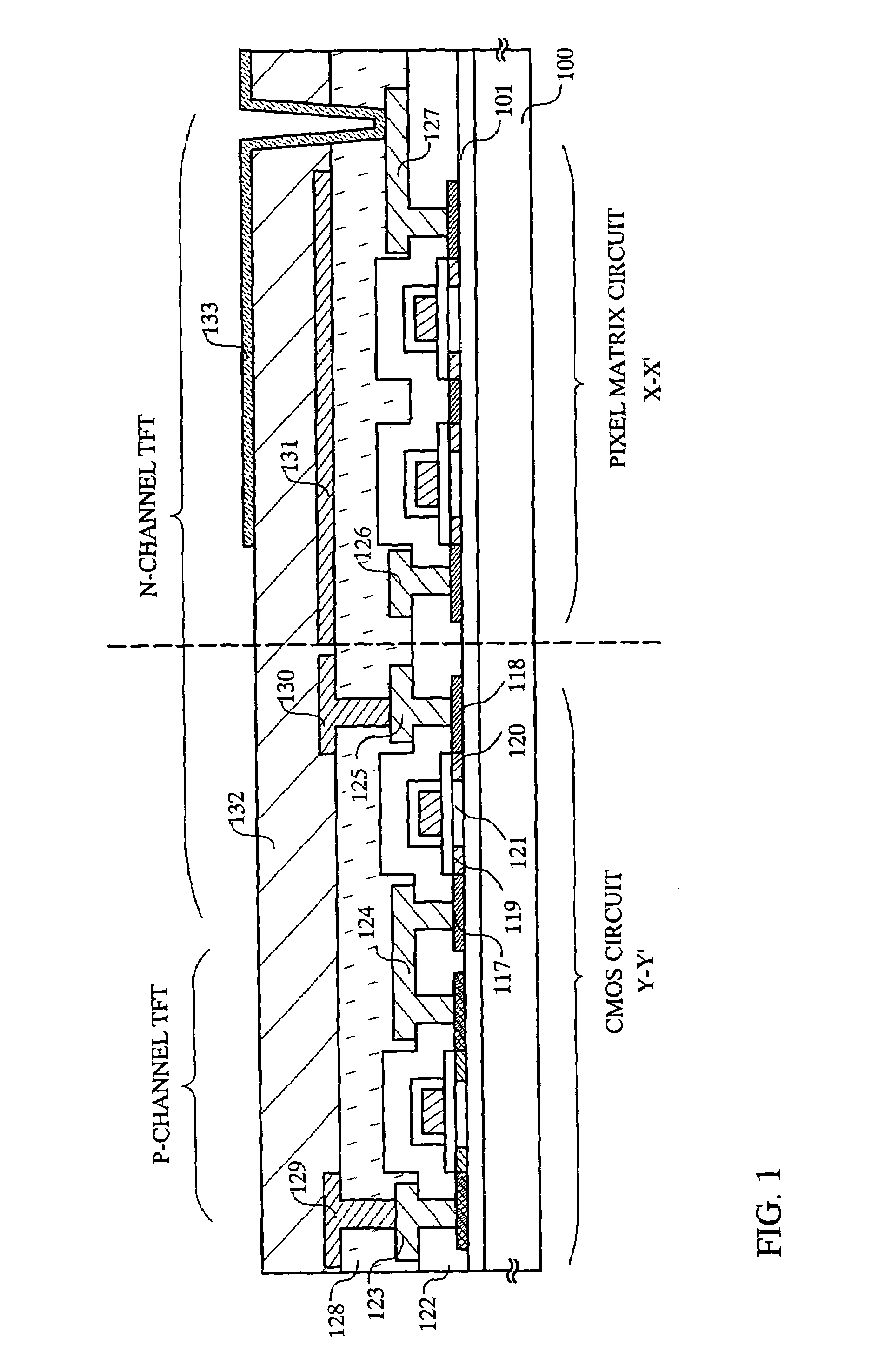
[0087]In this embodiment, a description will be made on an example in which a CMOS circuit, that is a part of a peripheral drive circuit, and a pixel TFT, that is a part of a pixel matrix circuit, are formed on the single same substrate using the present invention. The semiconductor device and its manufacturing method will be described briefly with reference to the simple cross sectional drawings shown in FIGS. 1 to 6B.

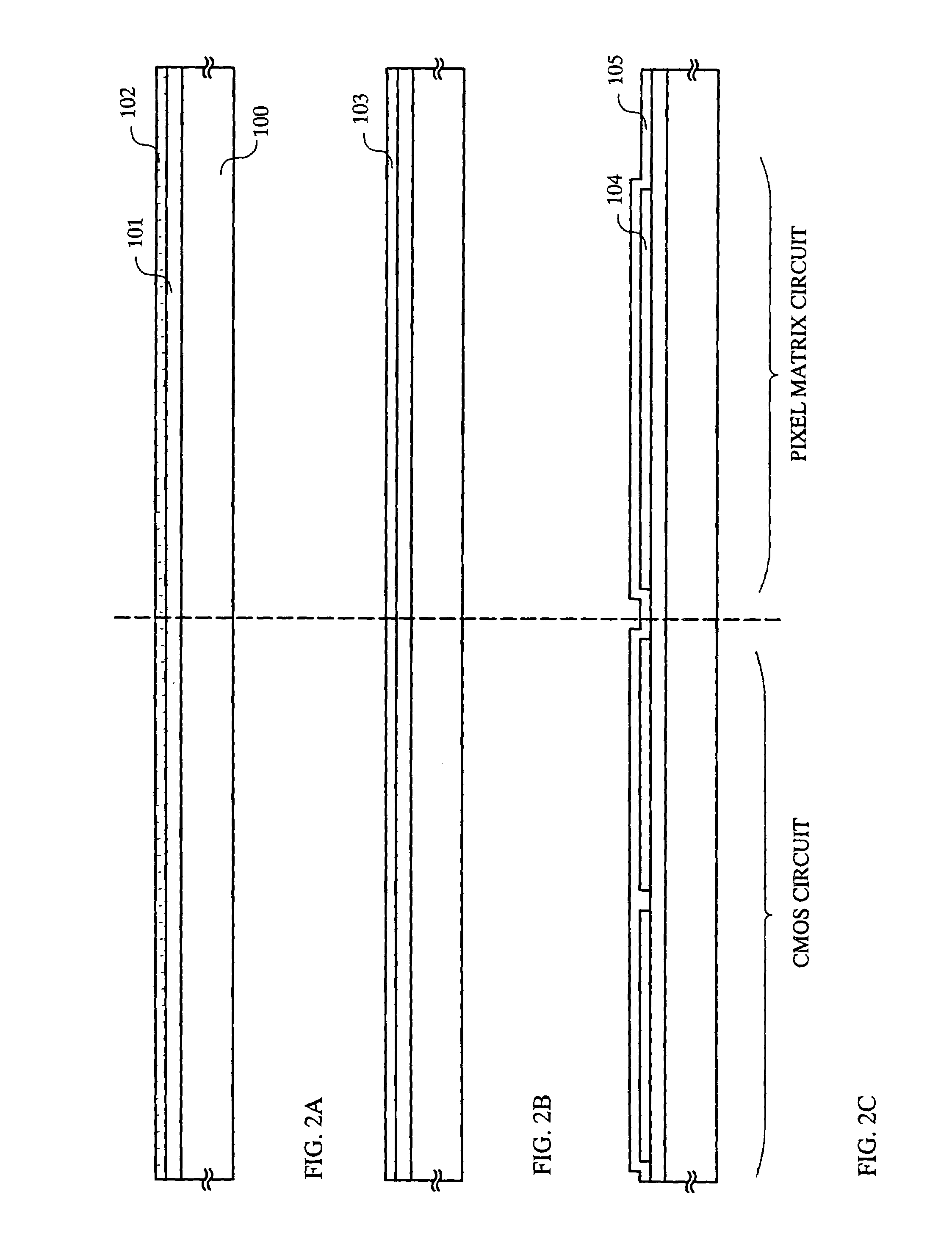
[0088]First the substrate 100 is prepared. In this embodiment, a glass substrate (Corning 1737, distortion point 667° C.) is used. Next, after a base insulating film (hereinafter in this specification, referred to as base film) is formed on top of the substrate 100, it is annealed. The heat treatment here is performed below the distortion point of the substrate, preferably between 200 and 700° C. In Embodiment 1, TEOS and oxygen (O2) are used as raw material gasses in a plasma CVD apparatus in order to form a 200 nm thick silicon oxide film as the base film 101, which...

embodiment 2

[0111]This embodiment takes an example in which a process that differs from that of Embodiment 1 is used to obtain a crystalline semiconductor film. In Embodiment 2 an additional process is performed before or after formation of the semiconductor film of Embodiment 1, which places a catalytic element either selectively or over the entire semiconductor surface, in order to promote crystallization. The basic structure of Embodiment 2 is similar to that of Embodiment 1, therefore the focus of the description will be on the differences only.

[0112]Embodiment 2 is the same as Embodiment 1 through the process of forming the semiconductor film by sputtering.

[0113]A catalytic element to promote silicon crystallization is introduced into the semiconductor film surface in Embodiment 2. Elements Ni, Fe, Co, Pt, Cu, Au, and Ge may be used either singly, or in combination, as the catalyst for promoting silicon crystallization. Ni was chosen for Embodiment 2 due to its quick diffusion speed throug...

embodiment 3

[0118]This embodiment takes an example in which a process that differs from that of Embodiment 1 is used to obtain a crystalline semiconductor film. In Embodiment 1, after the heat treatment is given on the base film, a semiconductor film is formed by sputtering, but in Embodiment 3, the base film and the semiconductor film are formed in succession, without exposure to the atmosphere.

[0119]First, a plastic substrate is prepared. A silicon nitride film is formed on top of the substrate by sputtering to act as a base film, and an amorphous silicon film is laminated, also by sputtering, to act as a semiconductor film. The two films are formed in succession, without exposure to the atmosphere. It is possible to create a clean interface between the base film and the semiconductor film with this processing method.

[0120]Next, laser light irradiation is used to form a crystalline semiconductor film by crystallizing the amorphous silicon semiconductor film. Further, a gate insulating film ma...


PUM


Abstract

In the present invention, a semiconductor film is formed through a sputtering method, and then, the semiconductor film is crystallized. After the crystallization, a patterning step is carried out to form an active layer with a desired shape. The present invention is also characterized by forming a semiconductor film through a sputtering method, subsequently forming an insulating film. Next, the semiconductor film is crystallized through the insulating film, so that a crystalline semiconductor film is formed. According this structure, it is possible to obtain a thin film transistor with a good electronic property and a high reliability in a safe processing environment.

Description

[0001]This application is a divisional of application Ser. No. 09 / 412,512 filed Oct. 5, 1999, now abandoned.BACKGROUND OF THE INVENTION[0002]1. Field of the Invention[0003]The present invention relates to a semiconductor device including a semiconductor circuit comprising a semiconductor element, such as insulated gate type transistors, and a manufacturing method thereof. In particular, it relates to the technology for forming crystalline semiconductor films on top of insulating surfaces. The semiconductor device of the present invention is not limited to thin film transistors (TFTs), MOS transistor, and other insulated type gate transistor elements themselves, but instead include display devices, image sensors, and other electro-optical devices incorporating semiconductor circuits made from those insulated gate type transistors. In addition, the semiconductor device in the present invention includes electronic equipment incorporating the display devices or electro-optical devices.[...

Claims


Application Information

Patent Timeline
Patent Type & Authority Patents(United States)
IPC IPC(8): H01L33/00H01L21/77H01L21/84H01L27/12H01L27/32H01L51/52
CPCH01L27/1214H01L27/1274H01L51/5237H01L51/524H01L29/4908H01L27/3244H01L27/3262H01L27/3276H01L51/5259H10K59/1213H10K59/12H10K59/131H10K50/846H10K50/841H10K50/8426
Inventor YAMAZAKI, SHUNPEI
Owner SEMICON ENERGY LAB CO LTD
Why Eureka
Try Eureka