Silicon-containing polymer, negative type resist composition comprising the same, and patterning method for semiconductor device using the same

Inactive Publication Date: 2006-10-31
SAMSUNG ELECTRONICS CO LTD
View PDF6 Cites 1 Cited by
  • Summary
  • Abstract
  • Description
  • Claims
  • Application Information

AI Technical Summary

Benefits of technology

[0012]Also provided is a negative type resist composition that can be used in conjunction with KrF eximer laser (248 nm), ArF excimer laser (193 nm) and next-generation F2 excimer laser (157 nm), which also provides high dry etching resistance by including silicon and can be advantageously used in a BLR process to realize high resolution power and large aspect ratios.

Problems solved by technology

Such pattern size is difficult to achieve using conventional lithography processes using lower wavelength devices, e.g., a KrF eximer laser (248 nm), with a conventional resist material.
Further, conventional ArF or F2 resist materials suffer from a variety of drawbacks due to their structural limitation.
One problem is the increase in the occurrence of patterns collapsing as the aspect ratio of pattern features increases.
Another problem is the weak resistance against a dry etching process.
Although positive type chemically amplified resists are preferred in view of their higher resolution, compositions synthesized from the positive type chemically amplified resists suitable for the BLR process are too hydrophobic.
Thus, adhesion to underlying layer materials is weak, and it is difficult to control the amount of silicon needed to create suitable resist materials.
In particular, the most serious problem with the positive type chemically amplified resists is shrinkage by e-beam.
In pursuit of high-speed, highly-efficient DRAMs, there is a limitation in using positive type resists for forming isolated patterns.

Method used


Image

  • Silicon-containing polymer, negative type resist composition comprising the same, and patterning method for semiconductor device using the same
  • Silicon-containing polymer, negative type resist composition comprising the same, and patterning method for semiconductor device using the same
  • Silicon-containing polymer, negative type resist composition comprising the same, and patterning method for semiconductor device using the same

Examples


example 1

Synthesis of Polymer

[0056]

[0057]4.3 g of 3-[tris(trimethylsilyloxy)silyl]propyl methacrylate (10 mmol) and 3.9 g of 2-hydroxyethyl methacrylate (30 mmol) were dissolved in a round bottom flask containing 35 g of tetrahydrofuran (THF) and 0.33 g of azobisisobutyronitrile (AIBN) (5 mol %) and purged using nitrogen, followed by polymerizing at about 65° C. for about 12 hours.

[0058]After polymerization, the reactant was slowly precipitated with excess n-hexane. Thereafter, the precipitate was filtered, and the filtrate was dissolved in an appropriate amount of THF and re-precipitated in n-hexane. Then, the obtained precipitate was dried in a vacuum oven at about 50° C. for about 24 hours, giving a desired product at a yield of about 75%.

[0059]The obtained product had a weight average molecular weight (Mw) of about 13,200 and polydispersity (Mw / Mn) of about 1.9.

example 2

Synthesis of Polymer

[0060]

[0061]1.8 g of 4-hydroxystyrene (15 mmol), 2.0 g of 2-hydroxyethyl methacrylate (15 mmol), and 4.3 g of 3-[tris(trimethylsilyloxy)silyl]propyl methacrylate (10 mmol) were dissolved 30 g of THF and 0.33 g of AIBN (5 mol %), followed by polymerizing, thereby synthesizing a desired polymer at a yield of about 70%.

[0062]The obtained product had a weight average molecular weight (Mw) of about 12,100 and polydispersity (Mw / Mn) of about 2.0.

example 3

Synthesis of Polymer

[0063]

[0064]2.6 g of 2-hydroxyethyl methacrylate (20 mmol), 2.95 g of maleic anhydride (30 mmol) and 4.3 g of 3-[tris(trimethylsilyloxy)silyl]propyl methacrylate (10 mmol) were dissolved in 20 g of THF and 0.20 g of AIBN (2 mol %), followed by polymerizing, thereby synthesizing a desired polymer at a yield of about 50%.

[0065]The obtained product had a weight average molecular weight (Mw) of about 9,700 and polydispersity (Mw / Mn) of about 1.9.


PUM

PropertyMeasurementUnit
Percent by massaaaaaaaaaa
Weightaaaaaaaaaa
Molecular weightaaaaaaaaaa

Abstract

A polymer used for a negative type resist composition having a first repeating unit of a Si-containing monomer unit, a second repeating unit having a hydroxy group or an epoxy ring and copolymerized with the first repeating unit is provided. The first repeating unit is represented by the following formula:wherein R1 is a hydrogen atom or a methyl group, X is a C1–C4 alkyl or alkoxy group, and n is an integer from 2 to 4. Also, there is provided a negative type resist composition including the polymer which is an alkali soluble base polymer, a photoacid generator and a crosslinking agent cross linkable in the presence of an acid.

Description

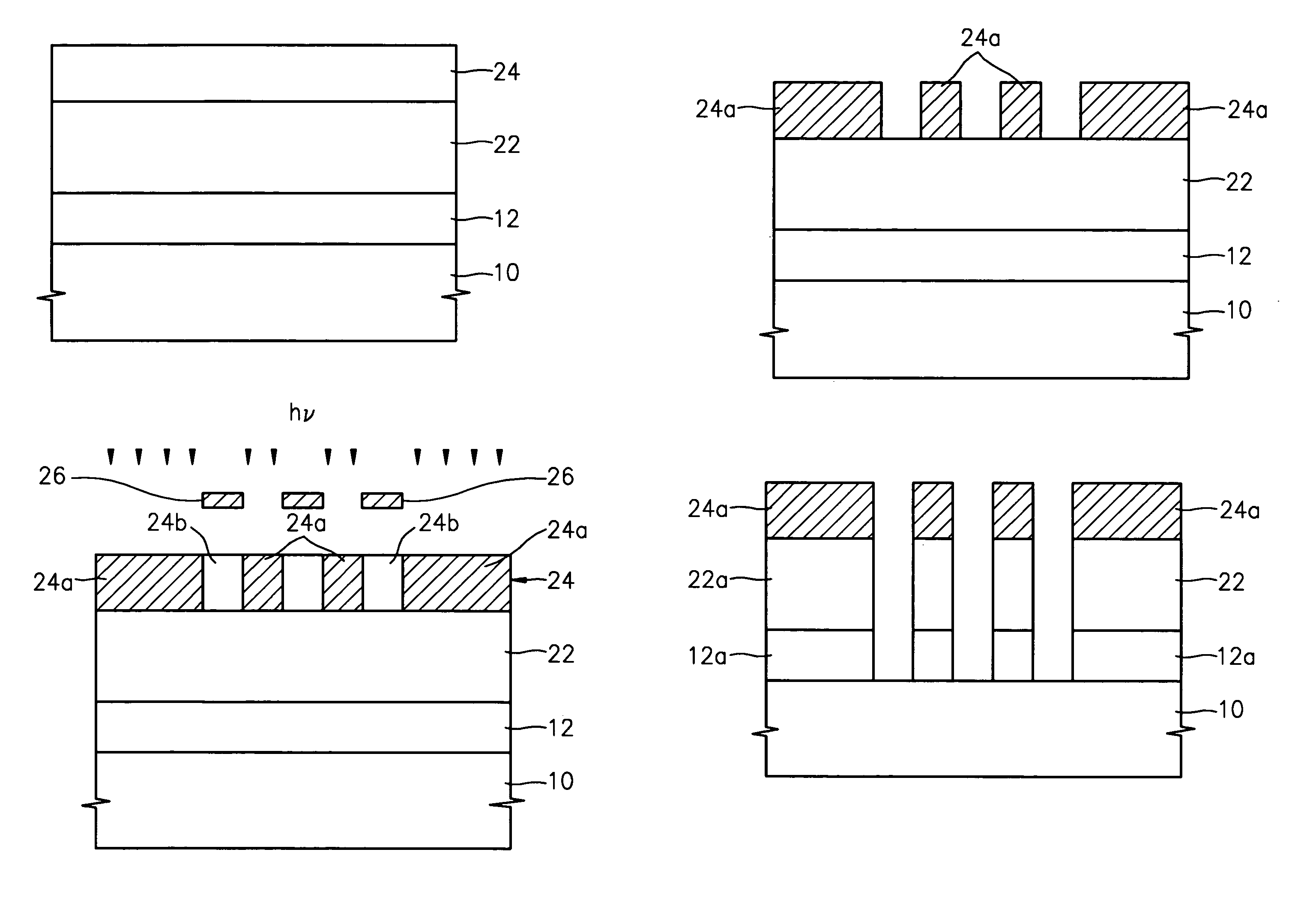
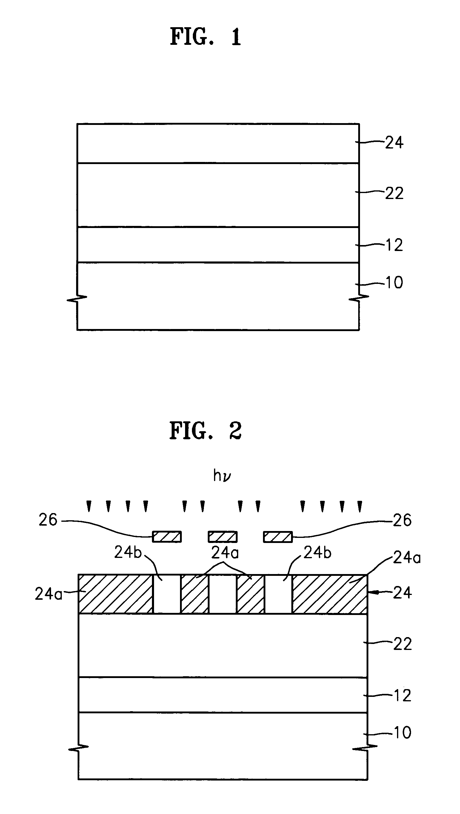
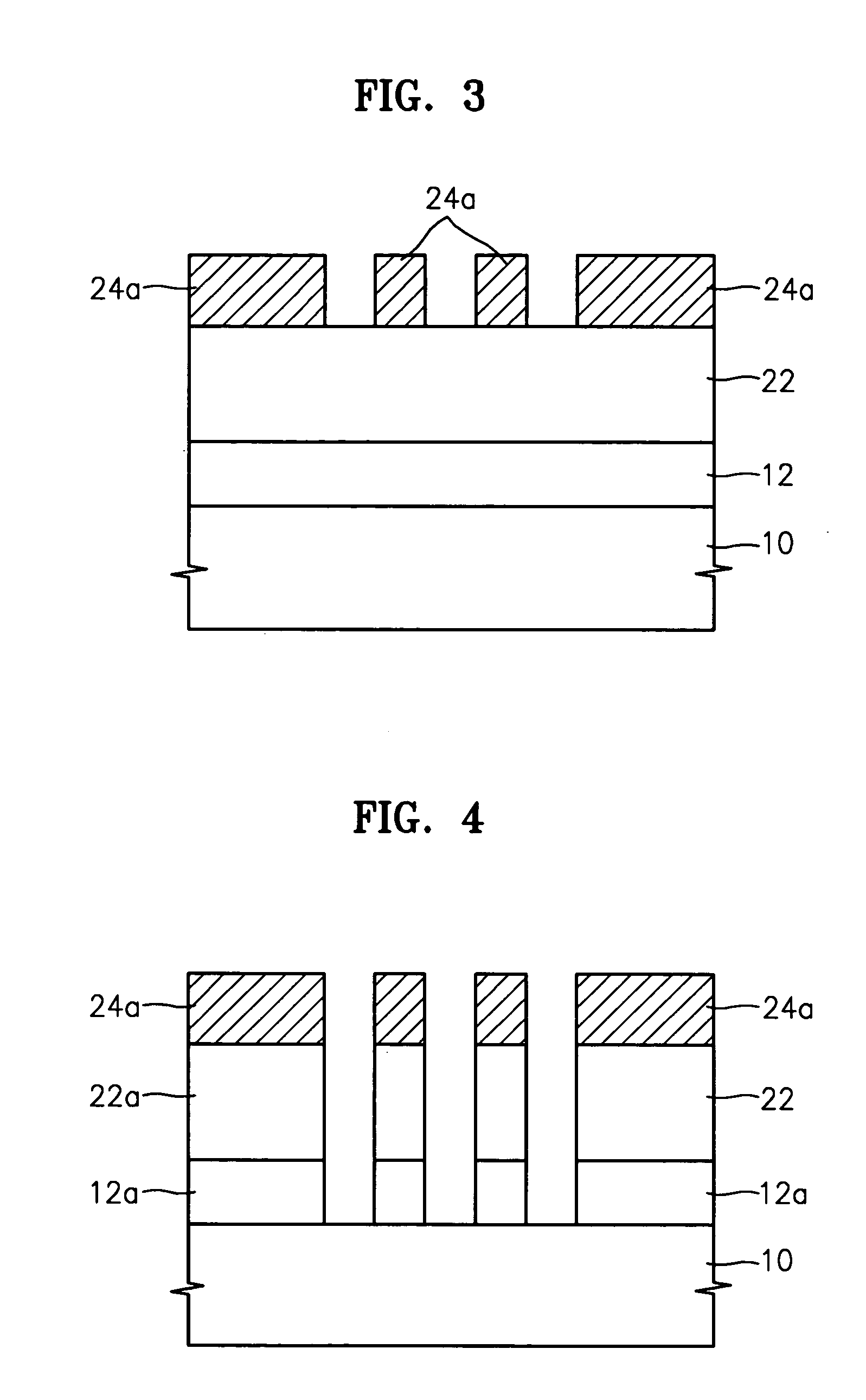
BACKGROUND[0001]1. Technical Field[0002]The present invention relates generally to silicon-containing polymers, negative type resist compositions comprising the same, and a patterning method for semiconductor devices using the same. More particularly, the present invention relates to silicon-containing polymers for use in a bi-layer resist (BLR) process, negative type resist compositions comprising the same, and a patterning method for semiconductor devices using the same.[0003]2. Discussion of the Related Art[0004]As semiconductor devices become more highly integrated and complex, the ability to form ultra-fine patterns becomes more important. For instance, in semiconductor devices of 1-Gigabit or greater, a pattern size having a design rule of 0.2 μm or less is needed. Such pattern size is difficult to achieve using conventional lithography processes using lower wavelength devices, e.g., a KrF eximer laser (248 nm), with a conventional resist material. Lithography processes using ...

Claims


Application Information

Patent Timeline
IPC IPC(8): G03C1/73C08F30/08G03F7/038G03F7/30G03F7/36G03F7/38G03F7/075G03F7/095
CPCC08F220/26C08F230/08G03F7/0382G03F7/0758G03F7/095Y10S430/146Y10S430/122Y10S430/111Y10S430/126Y10S430/115C08F230/085G03F7/075
Inventor CHOI, SANG-JUN
Owner SAMSUNG ELECTRONICS CO LTD
Why Eureka
Try Eureka