Inspection system by charged particle beam and method of manufacturing devices using the system

Inactive Publication Date: 2006-11-14
EBARA CORP
View PDF53 Cites 56 Cited by
  • Summary
  • Abstract
  • Description
  • Claims
  • Application Information

AI Technical Summary

Benefits of technology

[0160]The present invention has been completed on the basis of the problems as described above and has the object to provide an electron beam apparatus adapted to evaluate a sample at an improved throughput and with high reliability.
[0161]Another object of the present invention is to provide an electron beam apparatus with an improved charging detection function and at an improved reliability of evalua

Problems solved by technology

Therefore, the conventional apparatuses have the problem that a long period of time is required for inspection of a defect of a sample.
Moreover, they may present the problem that a quality SEM image cannot be obtained because a wafer with an insulating material disposed on the surface thereof is charged with electricity when the beam current is made larger in order to accomplish high throughput.
Further

Method used


Image

  • Inspection system by charged particle beam and method of manufacturing devices using the system
  • Inspection system by charged particle beam and method of manufacturing devices using the system
  • Inspection system by charged particle beam and method of manufacturing devices using the system

Examples


first embodiment

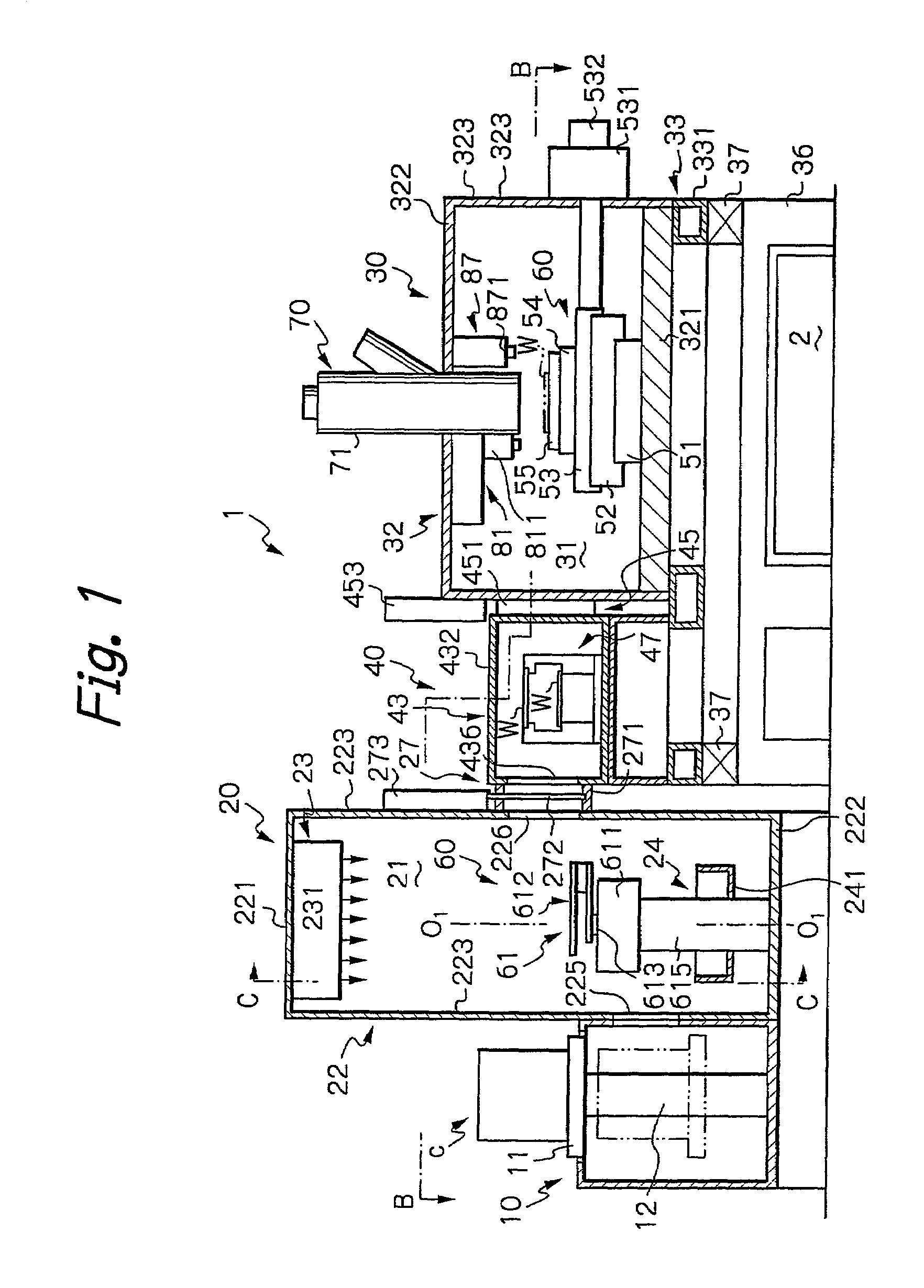
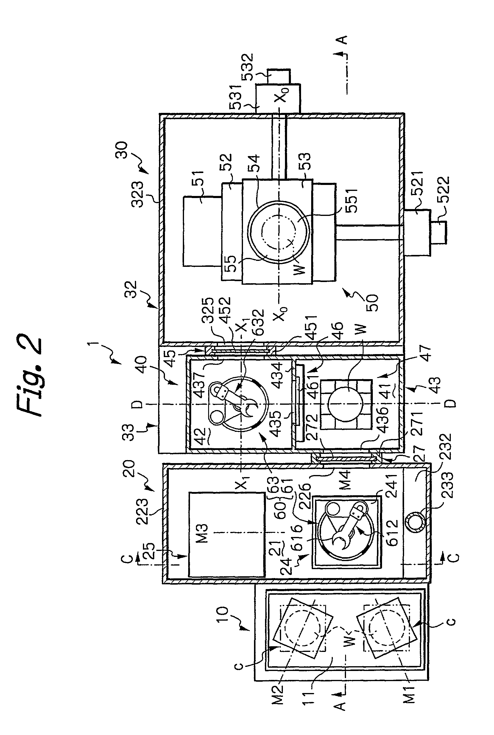
[0282]With reference to FIGS. 1 and 2, the present invention will be explained in the form of a semiconductor testing apparatus for testing, as an object under testing, a substrate, i.e., a wafer which has patterns formed on the surface thereof. FIGS. 1 and 2 illustrate main components of a semiconductor testing apparatus 1 according to this embodiment in elevation and a plan view, respectively.

[0283]The semiconductor testing apparatus 1 of this embodiment comprises a cassette holder 10 for holding cassettes which stores a plurality of wafers; a mini-environment device 20; a main housing 30 which defines a working chamber; a loader housing 40 disposed between the mini-environment device 20 and the main housing 30 to define two loading chambers; a loader 60 for loading a wafer from the cassette holder 10 onto a stage device 50 disposed in the main housing 30; and an electro-optical device 70 installed in the vacuum main housing 30. These components are arranged in a positional relati...

second embodiment

[0341]An operation of the electro optical apparatus (second embodiment in FIG. 7) with an above configuration will now be described. The primary electron beam emitted from the electron gun 721 is converged by the condenser lens 722 in the primary optical system 72 to form a crossover at a point P1. On the other hand, the primary electron beam converged by the condenser lens 722 passes through the plurality of apertures 723a of the multi-aperture plate to form into a plurality of primary electron beams, which are contracted by the minifying lens 724 so as to be projected onto a point P2. After being focused onto the point P2, the beams are further focused onto a surface of a wafer W by the objective lens 726. On the other hand, the deflecting system 727 disposed between the minifying lens 724 and the objective lens 726 deflects the primary electron beams so as to scan the surface of the wafer W.

[0342]The plurality of focused primary electron beams (nine beams in this embodiment) is i...

third embodiment

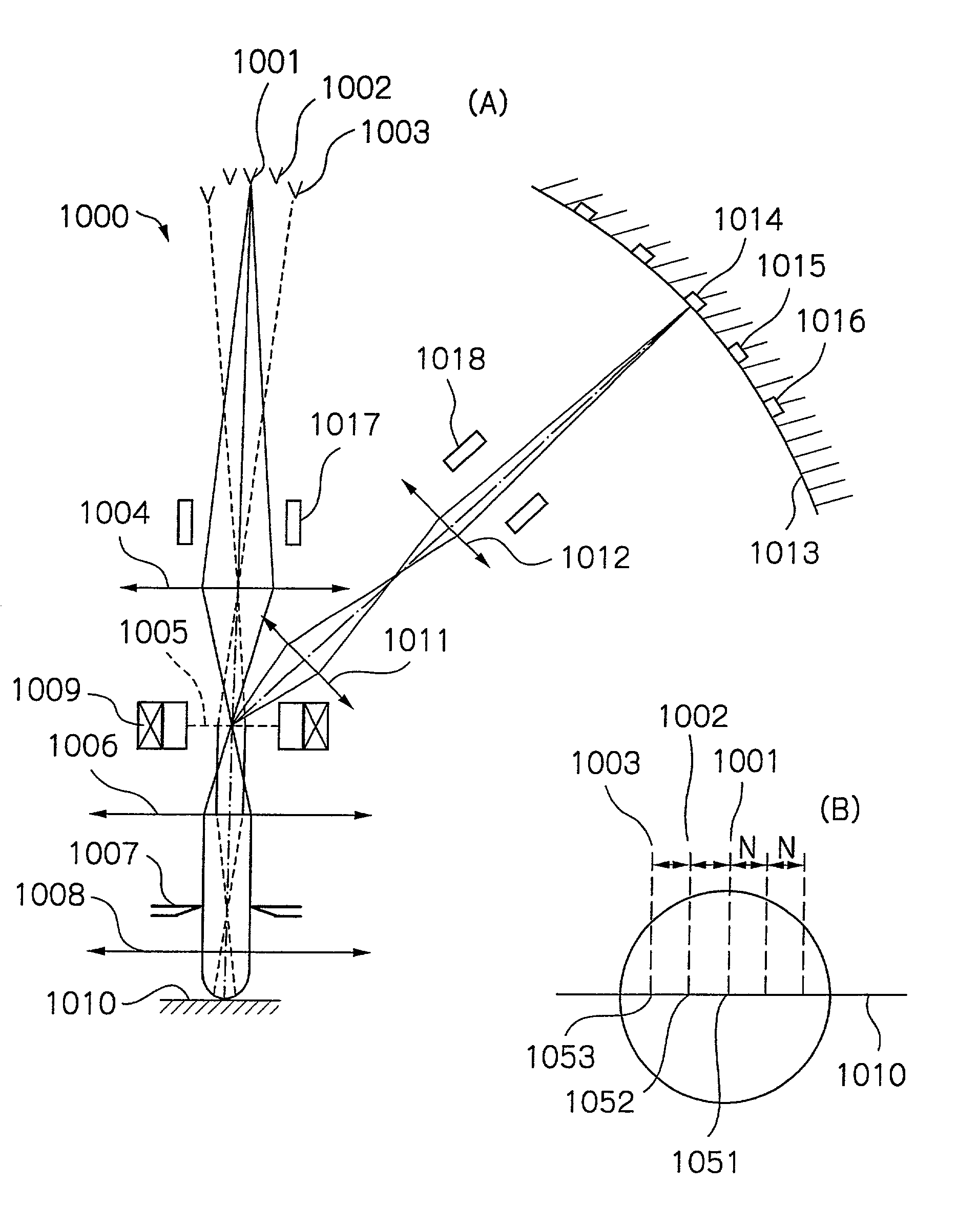
[0386]FIG. 14A is a schematic diagram of an optical system in an electron beam apparatus 1000 of a third embodiment according to the present invention. Primary electron beams emitted from multiple emitters 1001, 1002 and 1003 are converged by a condenser lens 1004 to be projected onto an image field 1005, which are further converged by a lens 1006 and an objective lens 1008 to be contracted and projected onto a sample surface 1010. Although FIG. 14A has illustrated only one row of multiple emitters, plural rows of emitters may be arranged as shown in FIG. 17A.

[0387]FIG. 17A shows emitters in the array of 3×3, and FIG. 17B is a cross sectional view taken along the line 17B-17B of FIG. 17A. In FIGS. 17A and 17B, reference numeral 1021 designates a Si substrate, 1022 is a Mo emitter, 1023 is an Au leading electrode, and 1024 is a Si3N4 insulating film. The number of emitters may be chosen appropriately. A lens unit has been constructed with a few numbers of planar electrodes each havin...


PUM


Abstract

An inspection apparatus and a semiconductor device manufacturing method using the same. The inspection apparatus is used for defect inspection, line width measurement, surface potential measurement or the like of a sample such as a wafer. In the inspection apparatus, a plurality of charged particles is delivered from a primary optical system to the sample, and secondary charged particles emitted from the sample are separated from the primary optical system and introduced through a secondary optical system to a detector. Irradiation of the charged particles is conducted while moving the sample. Irradiation spots of the charged particles are arranged by N rows along a moving direction of the sample and by M columns along a direction perpendicular thereto. Every row of the irradiation spots of the charged particles is shifted successively by a predetermined amount in a direction perpendicular to the moving direction of the sample.

Description

TECHNICAL FIELD[0001]The present invention relates to an inspection apparatus for the inspection of a defect, etc. of a pattern formed on a surface of an object of inspection by using a plurality of electron beams. More particularly, the present invention relates to an inspecting apparatus for inspecting a pattern or the like with high throughput, which is formed on the surface of an object of inspection on the basis of an image data that in turn is formed by irradiating the object of inspection with electrons and trapping secondary electrons varying in accordance with characteristics and shapes of the surface thereof, as in the case where a defect of a wafer is to be detected in the semiconductor manufacturing process. In addition, the present invention relates to a method for manufacturing devices with a high yield by using the inspection apparatus according to the present invention.[0002]The present invention is concerned with a charged particle beam apparatus for detecting secon...

Claims


Application Information

Patent Timeline
IPC IPC(8): H01J37/28G01N23/225H01J37/06H01J37/073H01J37/18H01J37/20H01J37/22H01J37/244
CPCG01N23/225H01J37/05H01J37/06H01J37/073H01J37/075H01J37/185H01J37/20H01J37/222H01J37/226H01J37/244H01J37/28G03F7/70616H01J2237/2817H01J2237/0435H01J2237/057H01J2237/06316H01J2237/082H01J2237/202H01J2237/20228H01J2237/204H01J2237/22H01J2237/2446H01J2237/24485H01J2237/24564H01J2237/248H01J2237/2482H01J2237/2806H01J2237/2816H01J37/29
Inventor NAKASUJI, MAMORUNOJI, NOBUHARUSATAKE, TOHRUKIMBA, TOSHIFUMISOBUKAWA, HIROSIYOSHIKAWA, SHOJIKARIMATA, TSUTOMUOOWADA, SHINSAITO, MUTSUMIHAMASHIMA, MUNEKITAKAGI, TORU
Owner EBARA CORP
Why Eureka
Try Eureka