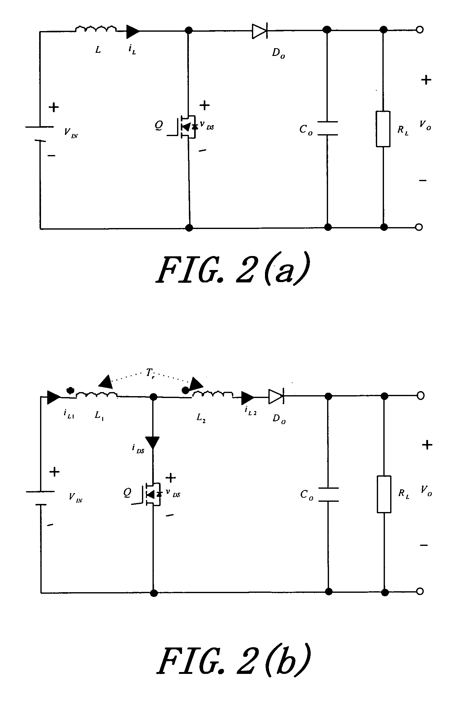
1. High output voltage boost ratio is achieved while only low turn ratio of winding for
coupling inductor and lenient duty cycles are needed. If the turn ratio of winding is too high, the primary and secondary winding can't be compacted tightly and coupling coefficient will decreases, which reduces output voltage; second, when the switch is turned on,
reverse bias voltage on secondary winding is proportional to DC input voltage multiplying the turn ratio of winding such that rectifying diodes have to bear this voltage plus output circuit's
high voltage. Increasing the turn ratio of winding can obtain relative low switch clamping voltage and lenient
duty cycle control while endurance of the
diode at high voltage side can not be solved easily, specially, when switching spike voltage from high voltage side winding; furthermore, if
duty cycle is too low induction current will be in non-continuous form and increases of ripples making current into see-saw waveforms, for example, since
MOSFET switch
conduction loss is proportional to the square of the current, under the same supplied power, see-saw current waveforms make higher switch loss than square waveforms. When duty cycle is close to one
conduction loss is improved, but the
diode at high voltage side has to endure the force of voltage and current.
First, since only a few moments to transfer all the energy, the
diode has to endure large
transient current; second, because above mentioned spike voltage problem, the switching duty cycle is too high, and the diode's capacity has to be increased such that the loss increases too. In a nutshell, increasing the turn ratio of winding to
gain high boost rate is not ideal.
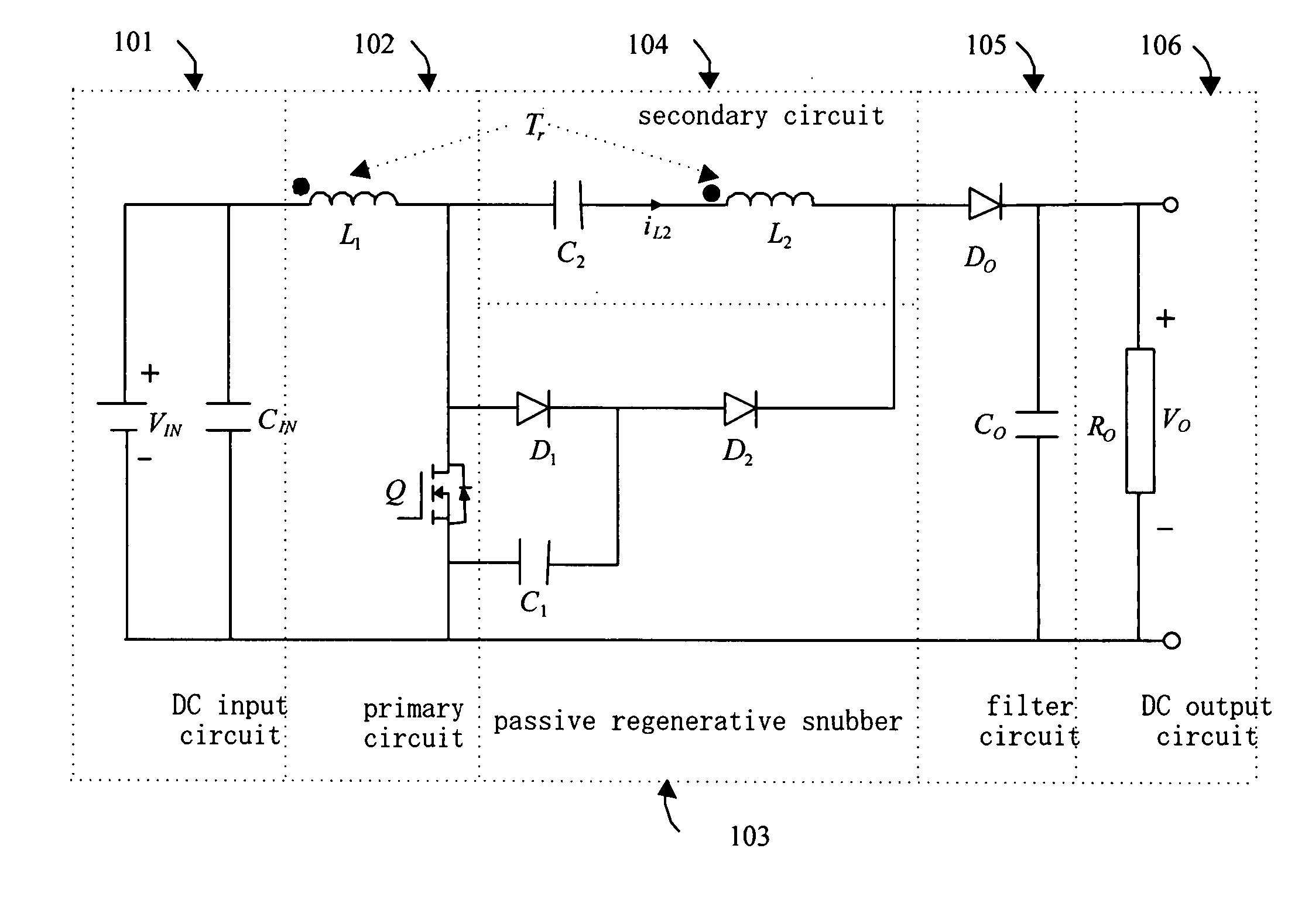
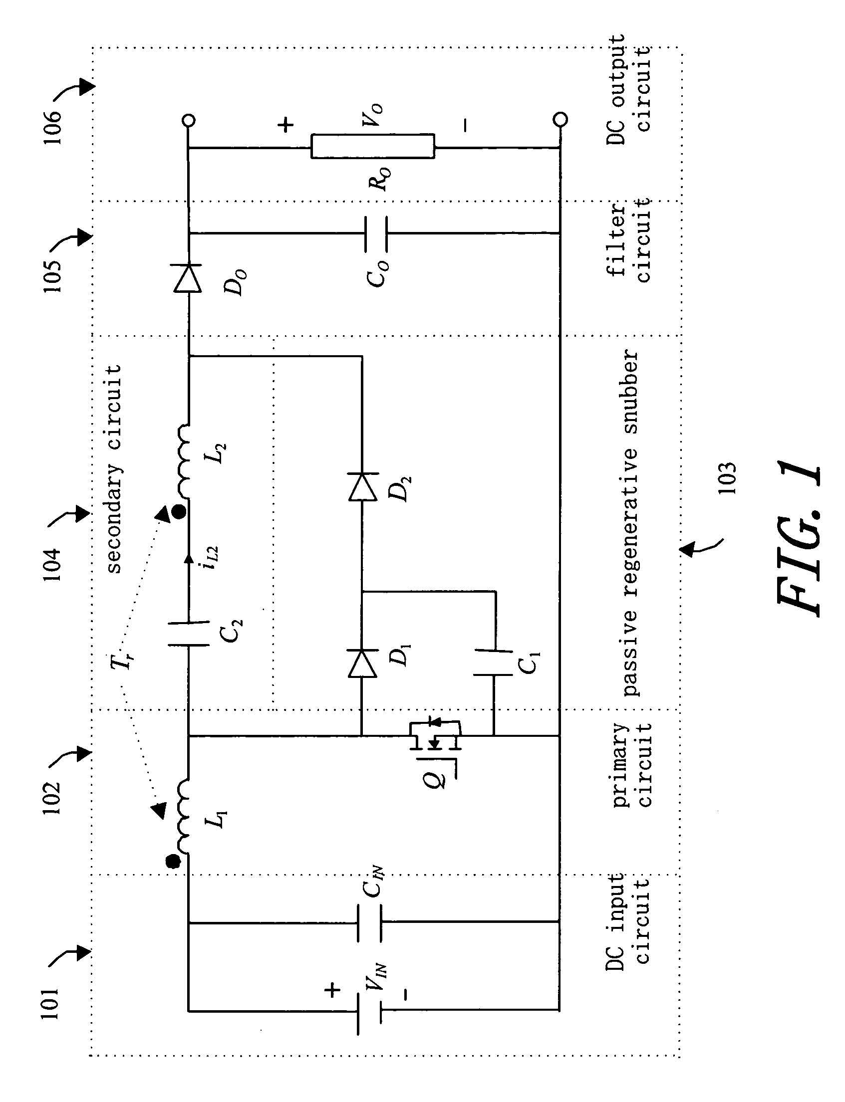
2. Passive regenerative
snubber can absorb circuit induction energy, which makes wire laying and production easy. Common used
snubber can be divided into three types: passive (consisting of
capacitor,
resistor and diode), active (auxiliary switch,
capacitor and diode) and passive regenerative (
capacitor and diode) and is mainly to absorb the energy caused by induction voltage (affecting voltage clamping) and reverse-
recovery current on the diode. The energy in the capacitor of the passive snubber is consumed completely by the
resistor, therefore it has lowest efficiency. The active snubber requires additional switch and
control circuit, other than internal circular current has to be addressed. The passive regenerative snubber first absorbs the energy affecting clamping voltage, and then transfer the energy to output terminal using original circuit; it requires lest components and increases a little in switching loss to build an auxiliary boosting circuit, as well has highest efficiency. The spike voltage is primarily caused by
high frequency of switching. Because power equals to voltage multiplying current, when current is very high at a
low voltage DC power source, spike voltage can be induced by a little distributed
inductance, which comes from improper wire
layout, inner induction of wire and components. To protect switch from being damaged by the spike voltage, a high capacity capacitor can be installed in parallel to the switch to clamp the voltage; in addition, spike current is quickly passed to passive regenerative snubber and there no high charging current and no
ripple voltage left such that both suppressions are achieved and clamping will not be affected even large circuit
inductance exists. Having a
high current and low induction wiring
layout can be a challenge in practice, and present circuit effectively reduces induction between wires.
3. The energy absorbed by the capacitor in passive regenerative snubber is applied to boost output voltage, and no circular current exists which further helps clamping voltage. The present invention not only transfers the energy from snubber to the output terminals, but also inserts voltage clamping in the process, further reducing voltage exerted on the switch and providing a key structure for bi-directional current return
route on secondary winding side.

