
Semiconductor device and a method of manufacturing the same

a technology of semiconductor devices and semiconductor devices, applied in the direction of transistors, basic electric elements, sustainable buildings, etc., to achieve the effect of reducing the on resistance (ron) and the feedback capacitance (cgd) of a power mosfet, improving the power added efficiency of a semiconductor device, and reducing the resistance of the sh

Active Publication Date: 2007-02-13
RENESAS ELECTRONICS CORP
View PDF17 Cites 20 Cited by
  • Summary
  • Abstract
  • Description
  • Claims
  • Application Information

AI Technical Summary

Benefits of technology

[0008]Of these, power MOSFETs are amplifying elements having a structure in which a drain is maintained at a high breakdown voltage by disposing, on a drain side, a heavily doped drain region via a lightly doped offset drain region. These elements are advantageous over compound semiconductor devices in providing easy bias control and high mass productivity, in spite of their inferiority in power added efficiency.
[0010]Accordingly, one of the problems of a semiconductor device for a mobile communication apparatus which uses a power MOSFET as an amplifying element is to improve the power added efficiency of an amplifier circuit using a power MOSFET. Another problem is to promote a size reduction of the chip on which a power MOSFET serving as an amplifying element is formed.
[0011]Improvement of the power added efficiency of an amplifying circuit can be attained by a reduction in the on resistance (Ron) of the power MOSFET and, at the same time, a reduction in the parasitic capacitance between the drain and gate, which is called a feedback capacitance (Cgd). There is however, a trade-off relationship between the on resistance (Ron) and the feedback capacitance (Cgd) of a power MOSFET. An increase in the impurity concentration of an offset drain region is effective for reducing the on resistance (Ron) of the power MOSFET. However, this inevitably increases the feedback capacitance (Cgd), which is a parasitic capacitance formed between the drain and gate, and lowers the power added efficiency of an amplifier circuit. It is therefore necessary to develop a technique that is capable of reducing both the on resistance (Ron and the feedback capacitance (Cgd) in order to improve the power added efficiency of a power MOSFET.
[0012]An object of the present invention is to provide a technique for improving the power added efficiency of a semiconductor device for use in mobile communication apparatuses.
[0028]The present invention makes it possible to reduce both the on resistance (Ron) and the feedback capacitance (Cgd) of a power MOSFET, leading to an improvement in the power added efficiency of a semiconductor device for mobile communication apparatuses.
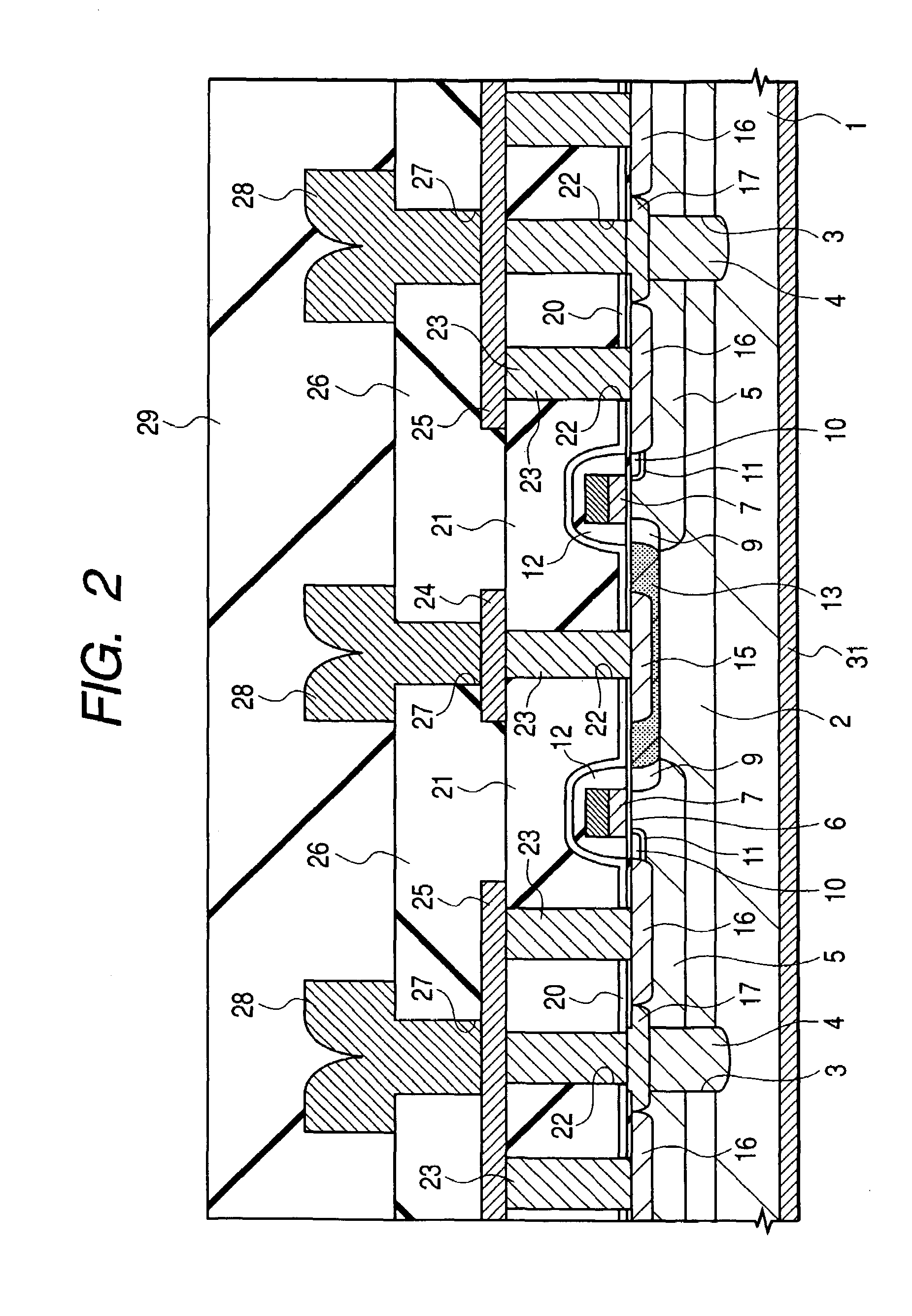
[0029]By shunting the gate electrode with a low-resistance plug made of a metal film embedded in a trench formed over the gate electrode of a power MOSFET and thereby reducing its sheet resistance, the provision of an Al alloy wiring region for a shunt becomes unnecessary, and the size of a semiconductor chip on which the power MOSFET is to be formed can be reduced.

Problems solved by technology

Accordingly, one of the problems of a semiconductor device for a mobile communication apparatus which uses a power MOSFET as an amplifying element is to improve the power added efficiency of an amplifier circuit using a power MOSFET.
Another problem is to promote a size reduction of the chip on which a power MOSFET serving as an amplifying element is formed.

Method used


Image

  • Semiconductor device and a method of manufacturing the same
  • Semiconductor device and a method of manufacturing the same
  • Semiconductor device and a method of manufacturing the same

Examples


embodiment 1

[0061]Embodiment 1 is a semiconductor device mounted on an RF (Radio Frequency) power module to be used for a digital mobile phone which transmits data by making use of, for example, a GSM system network.

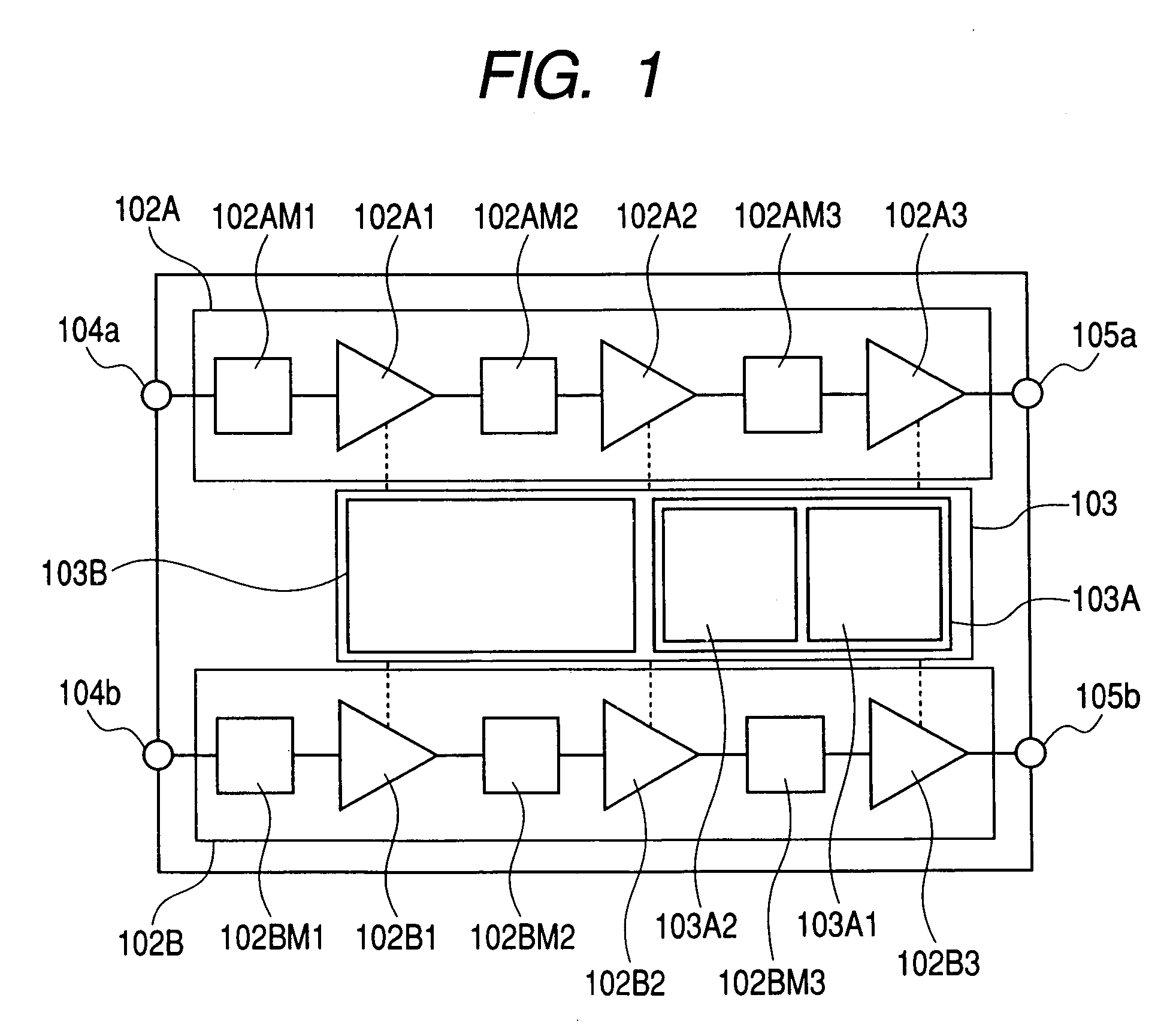
[0062]FIG. 1 is a block diagram of an amplifier circuit which constitutes the RF power module of Embodiment 1. In this diagram, there is illustrated an amplifier circuit to be used for an RF power module for which two frequency bands, for example, GSM900 and DCS1800, can be used (dual band system); and, at each frequency band, two communication systems, that is, a GMSK (Gaussian filtered Minimum Shift Keying) modulation system and an EDGE (Enhanced Data GSM Environment) modulation system, can be used.

[0063]The amplifier circuit has a power amplifier circuit 102A for GSM900, a power amplifier circuit 102B for DCS1800, and a peripheral circuit 103 which controls or assists the amplifying operation of each of the power amplifier circuits 102A and 102B. The power amplifier circuits 102A...

embodiment 2

[0106]In the power MOSFET according to Embodiment 1, a p type sinker layer 4 is formed by embedding a heavily doped p type polysilicon film inside of the trench 3. The p type sinker layer 4 formed by the present method is advantageous over a sinker layer formed by ion implantation of an impurity, because the parasitic resistance of the former one can be made lower than that of the latter one.

[0107]However, formation of the sinker layer by embedding a conductive film inside of the trench requires the digging of a deep trench in the substrate 1 so that it imposes many restrictions on the process and disturbs free disposal of the sinker layer. More specifically, for the formation of a sinker layer by embedding a trench with a conductive film, such as polysilicon film or metal film, a trench with a high aspect ratio is dug first, and, then, a conductive film is filled in the trench without a space. The appearance of voids in the conductive film inside of the trench disturbs the planariz...

embodiment 3

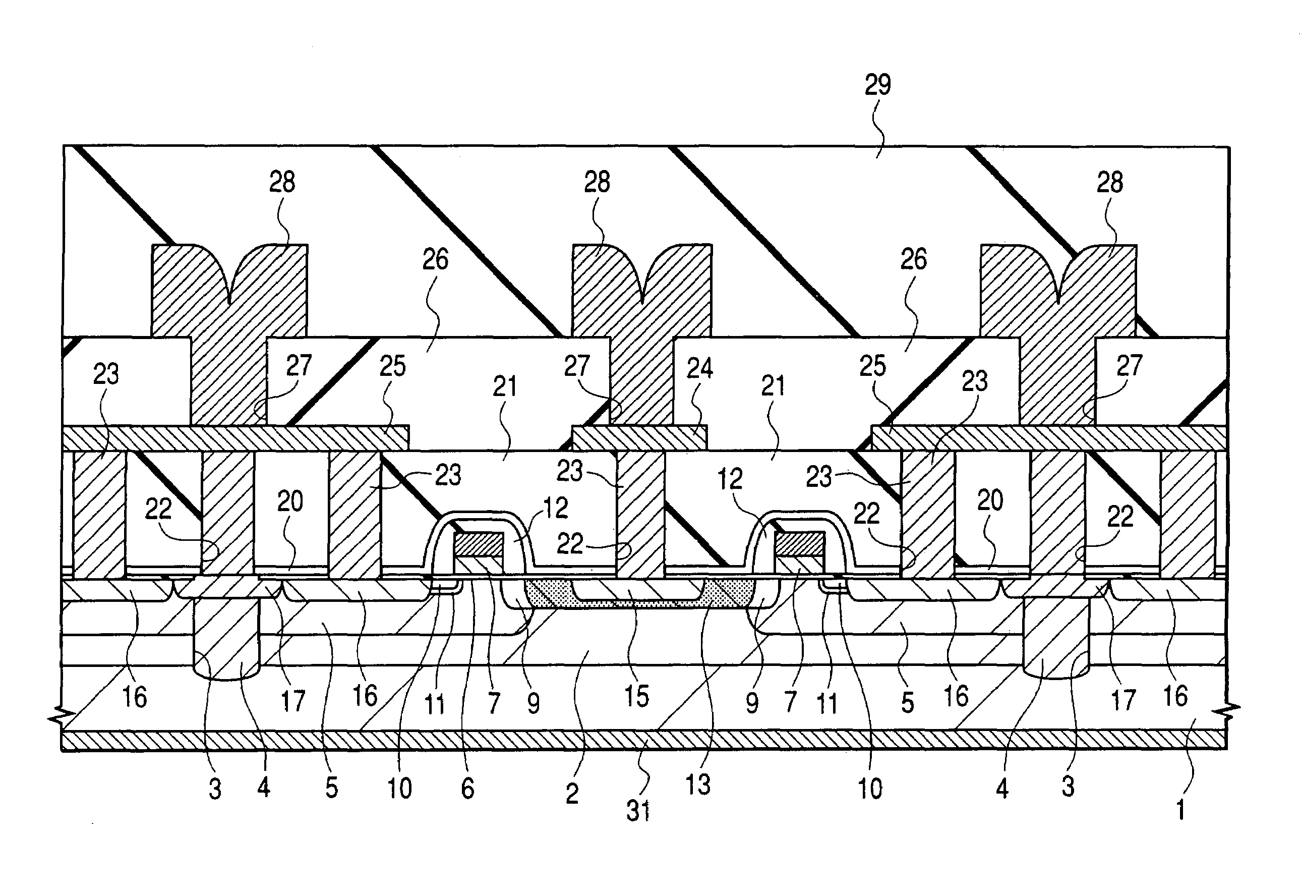
[0115]FIG. 27 is a fragmentary cross-sectional view of a substrate 1 illustrating a power MOSFET according to this Embodiment. In the n channel type power MOSFET of this Embodiment, a gate electrode 7 is composed only of an n type polysilicon film, a long trench 32 is formed in an insulating film over the gate electrode 7, and the gate electrode 7 is shunted by a plug 23 embedded inside of this long trench 32. The plug 23 is, similar to the plug 23 embedded inside of the contact hole 22, made of a metal film composed mainly of a W film. The long trench 32 has a length almost equal to that of the gate electrode 7 and extends in parallel to the gate electrode 7.

[0116]The long trench 32 over the gate electrode 7 is formed in the following manner. After deposition of a silicon oxide film 21 over the power MOSFET, the silicon oxide film 21 is dry etched using a photoresist film as a mask. Etching is once terminated on the surface of the silicon nitride film 21 covering the upper portion ...


PUM


Abstract

To reduce the size and improve the power added efficiency of an RF power module having an amplifier element composed of a silicon power MOSFET, the on resistance and feedback capacitance, which were conventionally in a trade-off relationship, are reduced simultaneously by forming the structure of an offset drain region existing between a gate electrode and an n+ type drain region of the power MOSFET into a double offset one. More specifically, this is accomplished by adjusting the impurity concentration of an n− type offset drain region, which is closest to the gate electrode, to be relatively low and adjusting the impurity concentration of an n type offset drain region, which is distant from the gate electrode, to be relatively high.

Description

CROSS-REFERENCE TO RELATED APPLICATION[0001]The present application claims priority from Japanese Patent application JP2003-313971, filed on Sep. 5, 2003, the content of which is hereby incorporated by reference into this application.BACKGROUND OF THE INVENTION[0002]The present invention relates to a semiconductor device to be used for mobile communication apparatuses (so called mobile phones) and to a technique for the manufacture thereof, particularly to a technique that is effective when applied to a semiconductor device to be mounted on an RF (Radio Frequency) power module.[0003]In recent years, mobile communication apparatuses (so called mobile phones), which employ a communication system typified by GSM (Global System for Mobile Communications), PCS (Personal Communication Systems), PDC (Personal Digital Cellular) system or CDMA (Code Division Multiple Access) system, have gained widespread use throughout the world.[0004]In general, such mobile communication apparatuses are ea...

Claims


Application Information

Patent Timeline
Patent Type & Authority Patents(United States)
IPC IPC(8): H01L29/76H01L27/01H01L27/12H01L29/94H01L21/3205H01L21/336H01L21/768H01L21/8234H01L23/367H01L23/522H01L23/66H01L27/06H01L27/088H01L29/08H01L29/41H01L29/417H01L29/423H01L29/49H01L29/78
CPCH01L21/823425H01L23/66H01L27/0629H01L27/088H01L29/66659H01L29/7835H01L23/3677H01L2924/1305Y02B60/50H01L2224/45144H01L2924/13091H01L24/48H01L29/0847H01L29/4175H01L29/41758H01L2224/48091H01L2224/48227H01L2924/01079H01L2924/19041H01L2924/19105H01L2924/3011H01L2924/00014H01L2924/00H01L24/45H01L29/0878
Inventor MIYAKE, TOMOYUKIMORIKAWA, MASATOSHIHOSHINO, YUTAKAHATORI, MAKOTO
Owner RENESAS ELECTRONICS CORP
Learn More