Light waveguide and fluorescent sensor using the light waveguide

a light waveguide and fluorescent sensor technology, applied in the field of light waveguides and fluorescent sensors using light waveguides, can solve the problems of complex configuration of fluorescent spectrophotometers, inability to reduce to such a size, and small fluorescent signal obtained, so as to achieve efficient guided and efficient excitation to the photodetector

Active Publication Date: 2007-02-20
TERUMO KK
View PDF15 Cites 22 Cited by
  • Summary
  • Abstract
  • Description
  • Claims
  • Application Information

AI Technical Summary

Benefits of technology

[0018]In consideration of the foregoing, it is an object of the present invention to provide a light waveguide such that fluorescence can be excited efficiently while suppressing the stray light arising from reflection of an excitation beam and that the fluorescent light generated can be efficiently guided to a photodetector.
[0019]It is another object of the present invention to provide a fluorescent sensor reduced in size to such an extent that the sensor can be utilized as an embedded-in-body type sensor, by use of this waveguide.

Problems solved by technology

However, the fluorescence spectrophotometer is complicated in configuration and, therefore, cannot be reduced to such a size as to be constantly connected to or embedded in a living body.
In the measurement using this sensor, however, it is difficult to homogeneously form an enzyme fixation film at the tiny optical fiber tip end, and the fluorescent light is diffused not only in the optical fiber direction but also in all directions, so that the fluorescent signal obtained is very small, and the photodetector needs to have a high amplification coefficient, as can be easily supposed.
This sensor, however, has difficulties in reducing the size of the argon laser utilized.
For example, it is difficult to achieve reductions in size and power consumption of an argon laser, as compared with the case of LED, and there is a limitation to reduction in overall size of the sensor inclusive of an optical system.
Until now, however, there has not yet been realized an apparatus by which the glucose concentration in a living body can be monitored accurately, continuously and for a long time.
In practice, however, stray light or the like due to the reflection arising from the difference in refractive index between layers or due to the reflection of light on wirings for supplying electric power to the LED (light source) and the photodetector is liable to be incident on the photodetector, and, even when an optical filter is used, the structure is difficult to realize for a sensor for measuring with high sensitivity the fluorescence which is faint relative to the excitation beam.
In this proposal, however, an angle must be formed between the direction of the LED light and the direction of the fluorescent light going toward the photodetector, so that a spacing for intersection of light beams must be provided between the LED and the photodetector and the sensor surface including the fluorescence indicator, resulting in that the overall size of the sensor would be enlarged and the efficiency of fluorescence detection might be worsened.

Method used


Image

  • Light waveguide and fluorescent sensor using the light waveguide
  • Light waveguide and fluorescent sensor using the light waveguide
  • Light waveguide and fluorescent sensor using the light waveguide

Examples


example 1

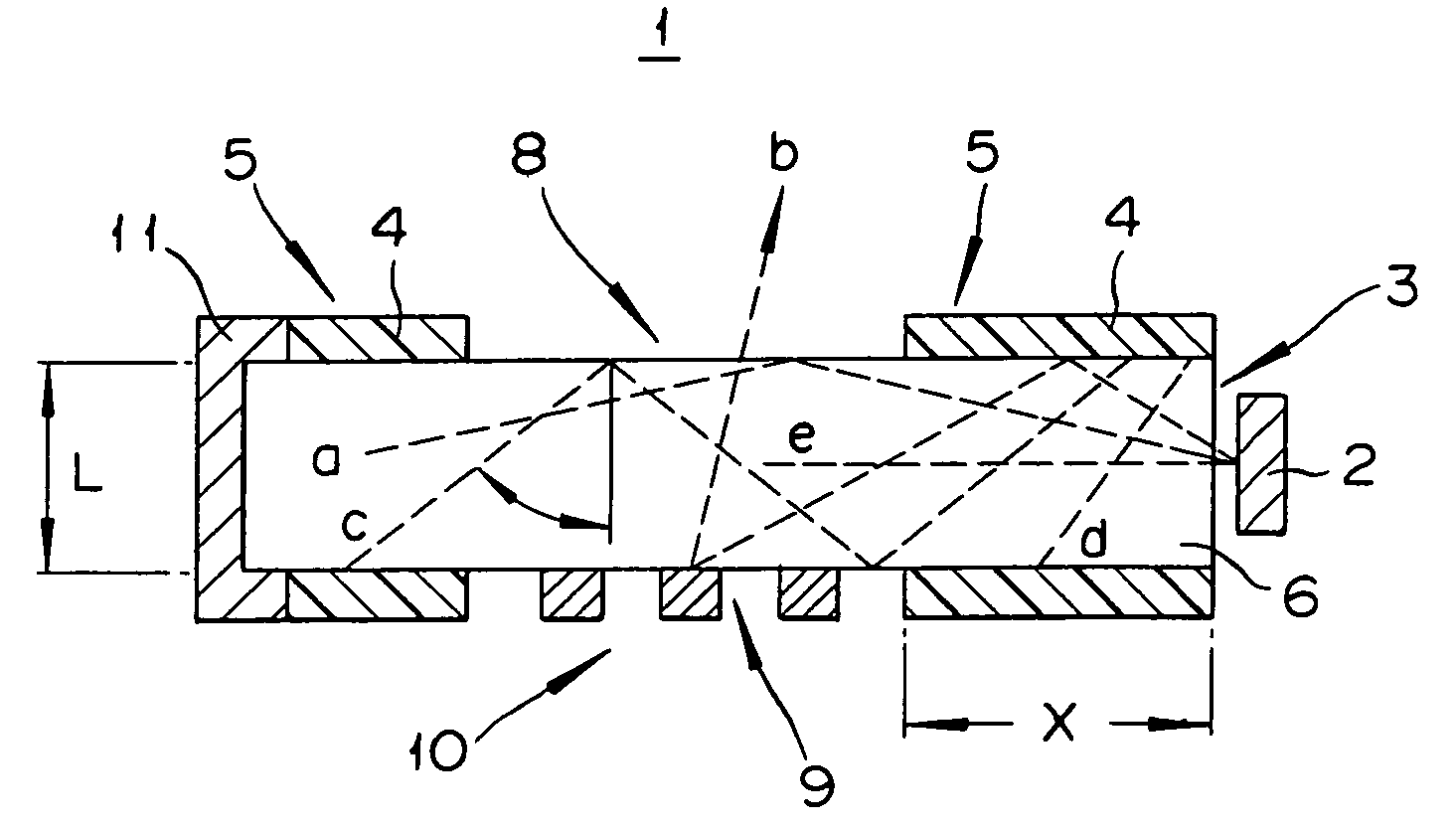
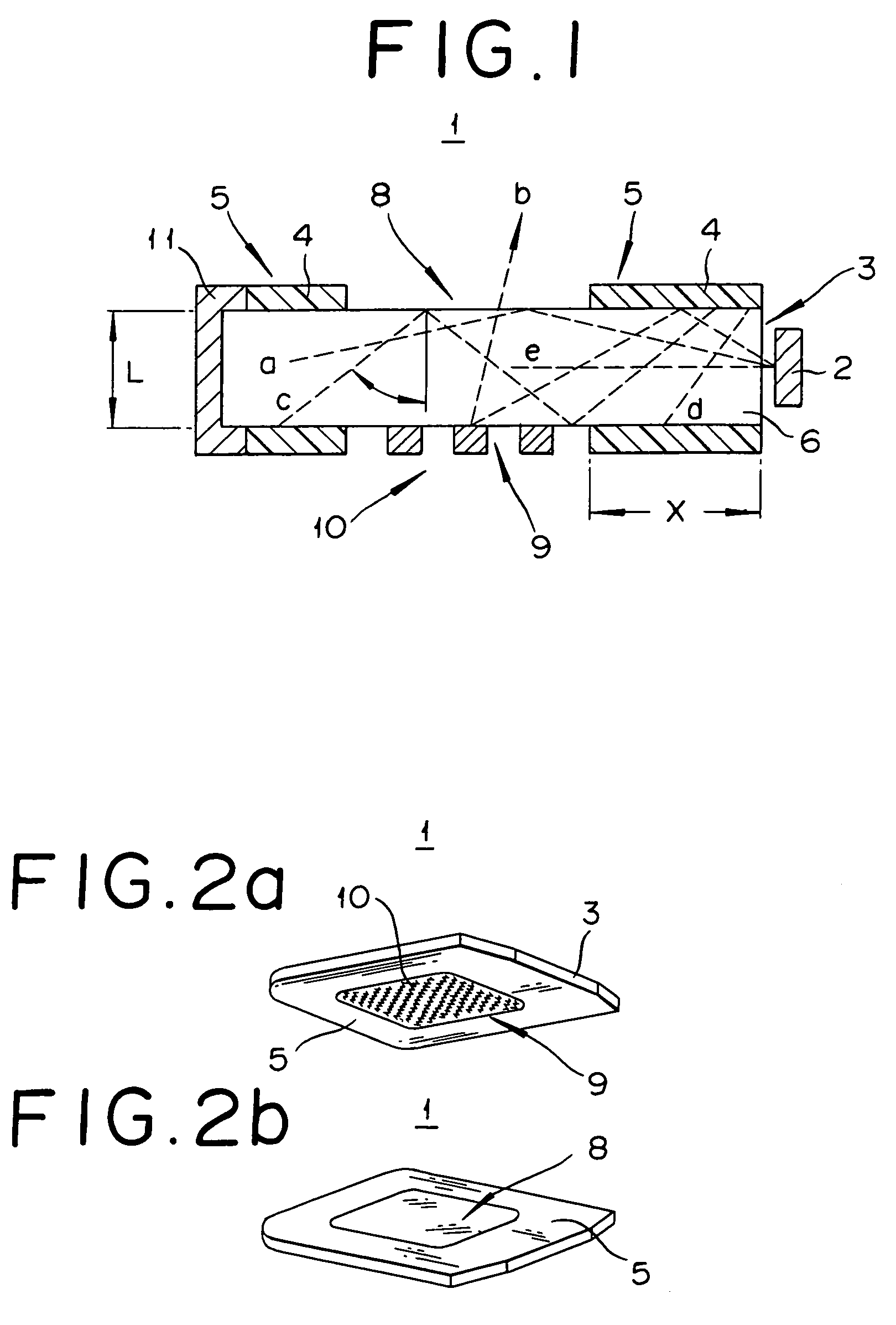
[0130]Example 1 pertains to a light waveguide 1 using a synthetic quartz plate (0.7 mm thick, 20 mm wide, 30 mm long; refractive index: 1.46; produced by Asahi Glass Co., Ltd.) as a waveguide main body 6.

[0131]In producing the light waveguide, first, a PET-based masking tape was adhered to one side of the synthetic quartz glass, and the masking tape was perforated. The holes were opened in the PET surface at a position spaced by at least 5 mm from an end portion of the synthetic quartz plate and in a 10 mm×10 mm region by use of an excimer laser. The holes had a diameter of 0.2 mm. The number of the holes opened in the 10 mm×10 mm region was 95, with a hole center interval of 1 mm.

[0132]In this case, masking may be conducted by use of a urethane resin dope or a styrene-based resin dope in place of the PET-based making tape, and only the resin portion may be similarly perforated by the excimer laser. Besides, the hole diameter can be controlled within the range of from 1 μm by regula...

example 2

[0142]Example 2 pertains to a light waveguide produced by use of a borosilicate glass plate (produced by Schott Corporation) having the same dimensions as those of the synthetic quartz plate shown in Example 1 as the waveguide main body 6.

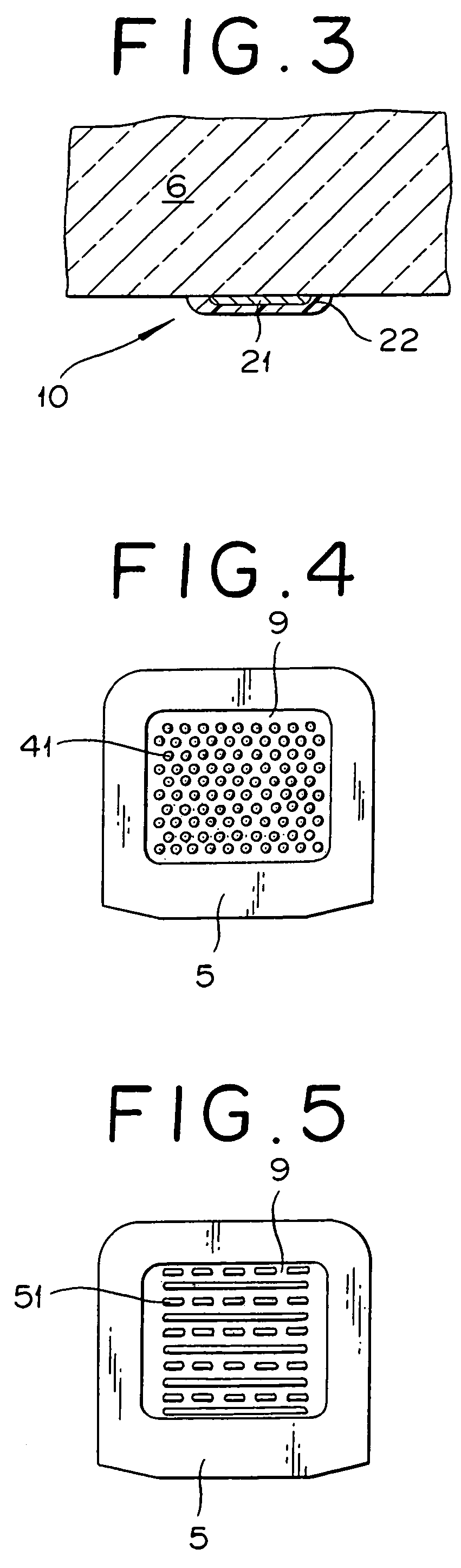
[0143]In producing the light waveguide, first, excimer laser (KrF; 280 mJ, 80 shots, 100 Hz) was radiated directly to the borosilicate glass plate, to produce holes with a hole diameter of 300 μm in the same pattern as in Example 1. The holes constitute recessed portions 61, the depth of which was 30 through 40 μm.

[0144]Subsequently, aluminum was sputtered by the same process as in Example 1, to produce an irregular reflection portion 10 with a diameter of 400 μm. The coverage of the light transmitting surface 9 with aluminum was 12%.

[0145]In Example 2, also, like in Example 1, the scattering of the wave-guided light from the whole area of the recessed portions 61 in the irregular reflection portion 10 could be recognized through the light radiatin...

example 3

[0146]Example 3 pertains to a fluorescent sensor 110 having a single window portion 112, produced by use of the light waveguide 1 produced in Example 2.

[0147]First, a light source 2 was disposed at a predetermined position in a housing 111, and was connected to the light waveguide 1. To obtain the light source 2, a 5 mmφ shot-type LED (produced by Sander Electronic Co., Ltd.) was machined so as to facilitate connection thereof to a side face of the waveguide, was adhered to a predetermined position in the housing by use of a commercially available black adhesive, and was connected to the light waveguide 1. In addition, a commercially available precision measurement photodiode (produced by Hamamatsu Photonics K.K.) with a 10 mm×10 mm measurement surface was connected to the absorption layer 4 in the periphery of the light transmitting surface of the light waveguide 1, with a commercially available optical filter (SC42; produced by Fuji Photo Film Co., Ltd.) therebetween, by use of a ...


PUM

PropertyMeasurementUnit
depthaaaaaaaaaa
diameteraaaaaaaaaa
diameteraaaaaaaaaa

Abstract

A light waveguide includes: a light introducing portion for introducing light coming from a light source into a waveguide main body; a light radiating surface for radiating the light introduced through the light introducing portion to the hydrogel side; a light transmitting surface which is disposed opposite to and in parallel to the light radiating surface and through which external light incident from the light radiating surface is transmitted to the exterior; a light separation portion, which provided on a surface in a region ranging from the light introducing portion to the light radiating surface and the light transmitting surface, reflecting only totally reflected components of the light introduced through the light introducing portion; an irregular reflection portion provided on the light transmitting surface to change the reflection angle on the light transmitting surface of the light reflected by the light separation portion; and a mirror portion provided at a position opposite to the light introducing portion.

Description

BACKGROUND OF THE INVENTION[0001]The present invention relates to a light waveguide and a fluorescent sensor using the light waveguide.DESCRIPTION OF THE RELATED ART[0002]Conventionally, a variety of analytical apparatuses have been developed as an apparatus for determining the concentration of an analyte in a liquid. For example, in one of such analytical apparatuses, several milliliters of a solution containing an analyte is put in a transparent vessel having a fixed capacity, the vessel is irradiated with appropriate light, and light absorption or fluorescence of the analyte is measured. This type of analytical apparatus is called a fluorescence spectrophotometer.[0003]The fluorescence spectrophotometer Fluorescence spectrophotometer is so designed that the irradiation axis of an excitation beam is set at 90° against the optical axis of the fluorescence to be measured, and, further, a prism and / or a diffraction grating is used to prevent the wavelength width of the excitation bea...

Claims


Application Information

Patent Timeline
Patent Type & Authority Patents(United States)
IPC IPC(8): G02B6/00G01N21/25
CPCG01N21/7703
Inventor MATSUMOTO, ATSUSHIIMUTA, SHUUJI
Owner TERUMO KK
Why Eureka
Try Eureka