Method of fabricating a semiconductor device having a decreased concentration of phosphorus impurities in polysilicon

a technology of phosphorus impurities and polysilicon, which is applied in the direction of semiconductor devices, basic electric elements, electrical equipment, etc., can solve the problems of reducing and affecting the miniaturization process. , to achieve the effect of greatly improving the adhesion strength between the polysilicon and the oxide film

Inactive Publication Date: 2007-03-06
PS4 LUXCO SARL
View PDF17 Cites 5 Cited by
  • Summary
  • Abstract
  • Description
  • Claims
  • Application Information

AI Technical Summary

Benefits of technology

[0007]As a result of investigation conducted by the inventors regarding process dependence of the fault, it has been found that a rate of fault occurrence greatly depends on a concentration of phosphorus in the polysilicon. It has also been found that the adhesion strength between the polysilicon and the oxide film can be greatly improved by reducing the concentration of phosphorus.
[0008]It is therefore an object of the present invention to provide a method for manufacturing a semiconductor device which is capable of greatly improving adhesion strength between a polysilicon and an oxide film.
[0015]Under such conditions, a bird's beak is formed in a lower end of the polysilicon during the thermal oxidation in the wet-hydrogen atmosphere. This bird's beak is formed so as to reduce a concentration of an electric field in the end of the polysilicon.
[0016]Phosphorus is doped at the aforementioned concentration so as to suppress a reduction in adhesion strength between the polysilicon and the gate oxide film caused by a stress of the bird's beak.

Problems solved by technology

In the polycide structure, further miniaturization is difficult due to a problem with resistance values.
However, a fault (or a defect) of peeling-off occurs between a gate polysilicon and a gate oxide film.
As a result of investigation, it has been discovered that a main cause of the fault is a reduction in adhesion strength between the polysilicon and the oxide film caused by wet-hydrogen oxidation.

Method used


Image

  • Method of fabricating a semiconductor device having a decreased concentration of phosphorus impurities in polysilicon
  • Method of fabricating a semiconductor device having a decreased concentration of phosphorus impurities in polysilicon
  • Method of fabricating a semiconductor device having a decreased concentration of phosphorus impurities in polysilicon

Examples


first embodiment

[0027]Now, description will be made of a semiconductor device according to a first embodiment of the present invention.

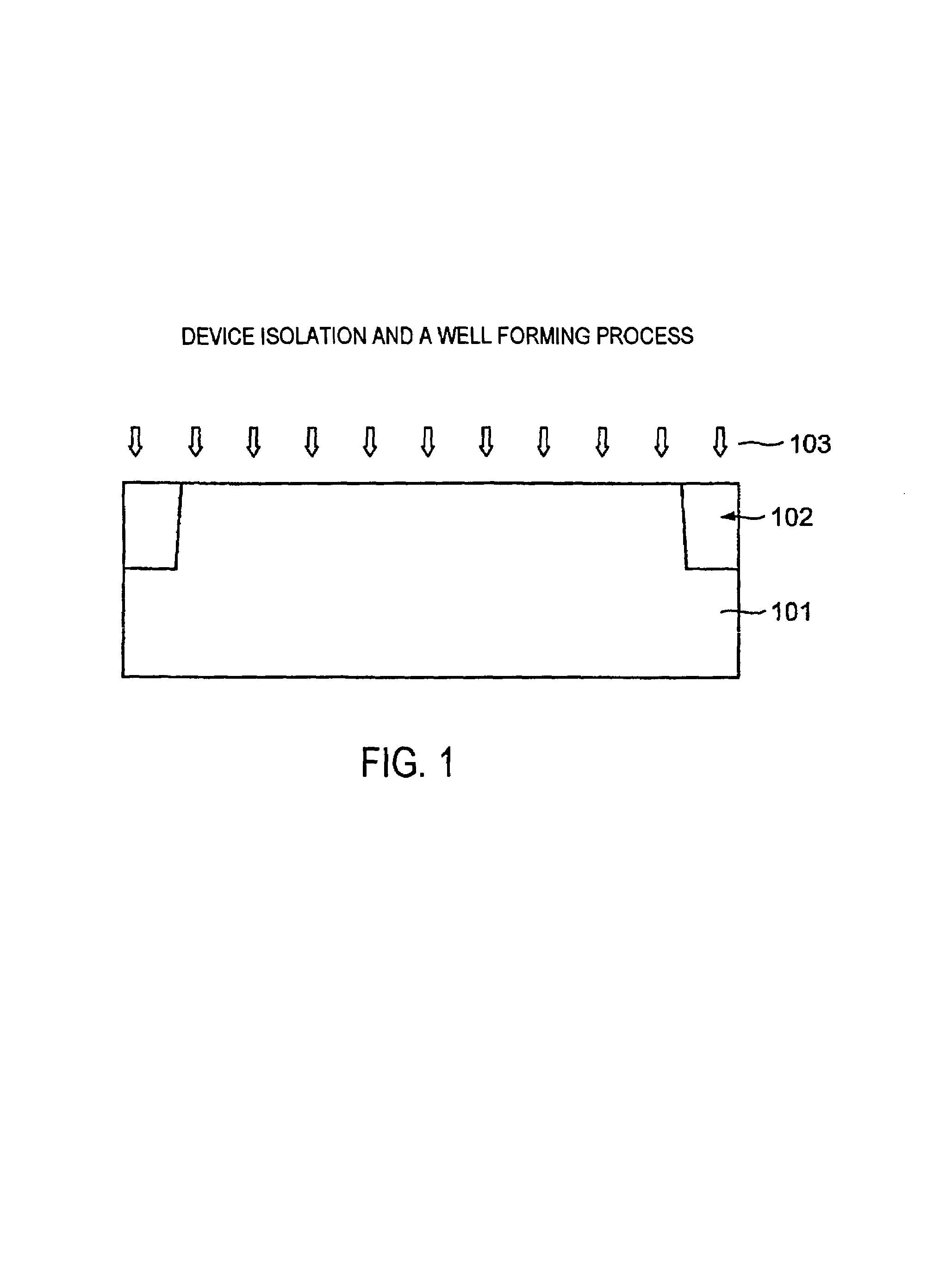
[0028]Referring to FIG. 1, a device isolation region 102 is formed in a silicon substrate 101. To provide device isolation, a shallow trench isolation (STI) to a depth of about 250 nm is generally used.

[0029]Then, impurities 103 are introduced into the silicon substrate 101 so as to form a well by ion implantation. When necessary, another ion implantation may be carried out in order to adjust a threshold of a MOS transistor. Such ion implantations are selectively carried out only in a desired region by photolithography.

[0030]Upon completion of such ion implantations, thermal treatment is performed at 900° C. for about 10 min.

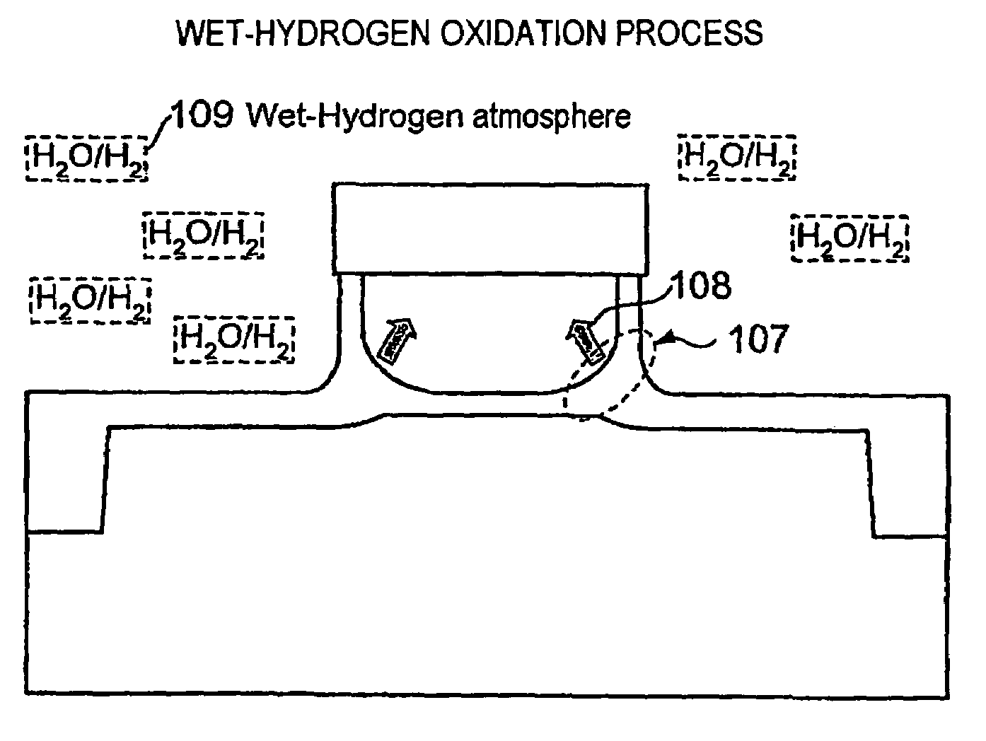
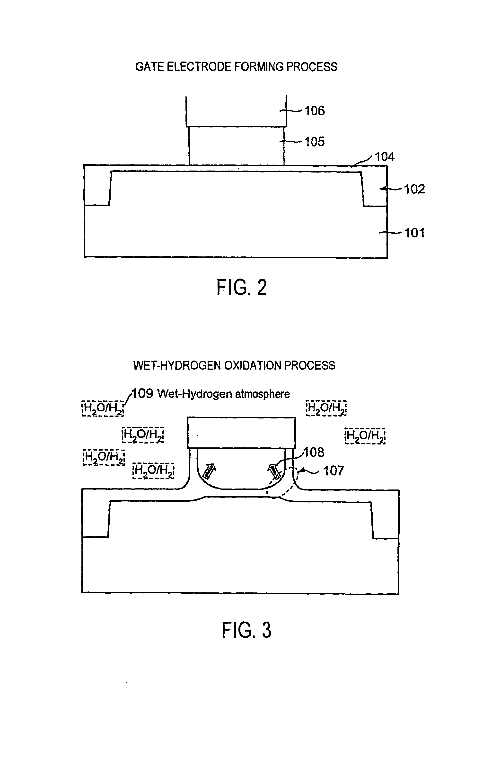
[0031]Subsequently, a gate electrode is formed. Referring to FIG. 2, a gate oxide film 104 having a thickness of about 7 nm is formed as a gate insulating film by a thermal oxidation method. Then, a phosphorus-doped polysilicon 105 and tungsten ...

second embodiment

[0047]Subsequently, description will be made of a semiconductor device according to a second embodiment of the present invention.

[0048]As shown in FIG. 7, in a phosphorus concentration distribution of a phosphorus-doped polysilicon 105, a low concentration is set in an interface side of a gate oxide film 104, and a high concentration is set in an interface side of tungsten 106. Adhesion strength in this case is similar to that shown in FIG. 6.

[0049]The high concentration is set in the tungsten 106 side in order to reduce interfacial resistance between the phosphorus-doped polysilicon 105 and tungsten 106. Also in this case, sufficiently large adhesion strength can be obtained compared with the phosphorus concentration of 4E20 (1 / cm3) in the polysilicon 105 according to the existing art. The adhesion strength is lower than with a uniform concentration of 1E20 (1 / cm3) of the first embodiment. This occurs because the phosphorus is redistributed in wet-hydrogen oxidation in a way which ...


PUM

PropertyMeasurementUnit
temperatureaaaaaaaaaa
thicknessaaaaaaaaaa
depthaaaaaaaaaa

Abstract

In a method for manufacturing a semiconductor device having a laminated gate electrode, a phosphorus-doped polysilicon is formed on a gate oxide film. A high-melting metal or a compound of a high-melting metal and silicon is formed on the polysilicon. Phosphorus is doped into the polysilicon so that a concentration of the phosphorus in the polysilicon at an interface between the polysilicon and the gate oxide film is 2×10²⁰(1 / cm3) or less. Then, thermal oxidation is carried out in a wet-hydrogen atmosphere containing water vapor.

Description

BACKGROUND OF THE INVENTION[0001]The present invention broadly relates to a method for manufacturing a semiconductor device having a laminated gate electrode.[0002]As a gate electrode of a next-generation MOS transistor, expectation is placed on a tungsten polymetal structure containing tungsten and a polysilicon. A tungsten polymetal gate has extremely low resistance compared with a currently mainstream tungsten polycide gate (laminated structure of a polysilicon and a compound of tungsten and silicon), and has the following advantages in a semiconductor integrated circuit.[0003]The first advantage is miniaturization. In the polycide structure, further miniaturization is difficult due to a problem with resistance values. This is because resistance values increase in inverse proportion to miniaturization in the same structure. By adopting the polymetal structure, it is possible to remove a barrier of the resistance value in miniaturization.[0004]The second advantage is the capabilit...

Claims


Application Information

Patent Timeline
Patent Type & Authority Patents(United States)
IPC IPC(8): H01L21/3205H01L21/4763H01L21/28H01L29/423H01L29/49H01L29/78
CPCH01L21/28247H01L21/28061H01L21/18
Inventor OGAWA, KAZUOOHYU, KIYONORIOKONOGI, KENSUKEIMAMURA, TOSHIHIROWATANABE, KEIICHIOHTA, HIROYUKI
Owner PS4 LUXCO SARL
Why Eureka
Try Eureka