Semiconductor quantum dot device

a quantum dot and semiconductor technology, applied in semiconductor devices, lasers, semiconductor lasers, etc., can solve the problems of reducing light emission efficiency, quantum dot lasers with operating speed exceeding that of semiconductor lasers, and structure or quantum well structure has not yet been proposed, so as to suppress the increase in the relaxation time of carriers

Inactive Publication Date: 2007-03-13
NEC CORP
View PDF5 Cites 6 Cited by
  • Summary
  • Abstract
  • Description
  • Claims
  • Application Information

AI Technical Summary

Benefits of technology

[0026]The quantum dot device of the present invention is a construction in which a p-type impurity is injected into quantum dots, whereby this p-type impurity causes the generation of holes inside the quantum dots, these holes being at the ground level of the valence band of the quantum dots. In such a construction, the relaxation of carriers (carrier injection) from an excited level to the ground level is accelerated, and increase in the relaxation time of the carriers is therefore suppressed. As a result, the modulation band of the quantum dot device can be extended and a broad modulation band on the order of 10 GHz or more and an operating speed on the order of 10 GHz or higher can be realized.

Problems solved by technology

However, these methods have the drawback that processing damage which occurs in the semiconductor crystal as a result of lithography or dry etching greatly reduces the light emission efficiency.
However, a quantum dot laser which has an operating speed surpassing that of a semiconductor laser of the prior art having an active layer of bulk structure or quantum well structure has not yet been proposed.
This is due to problems described hereinbelow that are inherent to quantum dots.
As a result, if the ground levels of the conduction band and valence band are already occupied by conduction electrons and holes (carriers), additional conduction electrons or holes cannot be injected in the ground level.
As is obvious from the foregoing explanation, the modulation rate in a quantum dot device such as a quantum dot laser drops due to decrease in the relaxation rate of carriers (increase in carrier relaxation time τ2-1), and this limited modulation rate complicates the realization of a modulation bandwidth on the order of 10 GHz, which is required in a current optical communication system.

Method used


Image

  • Semiconductor quantum dot device
  • Semiconductor quantum dot device
  • Semiconductor quantum dot device

Examples


examples

[0088]Explanation next regards examples of the present invention with reference to the accompanying drawing.

first example

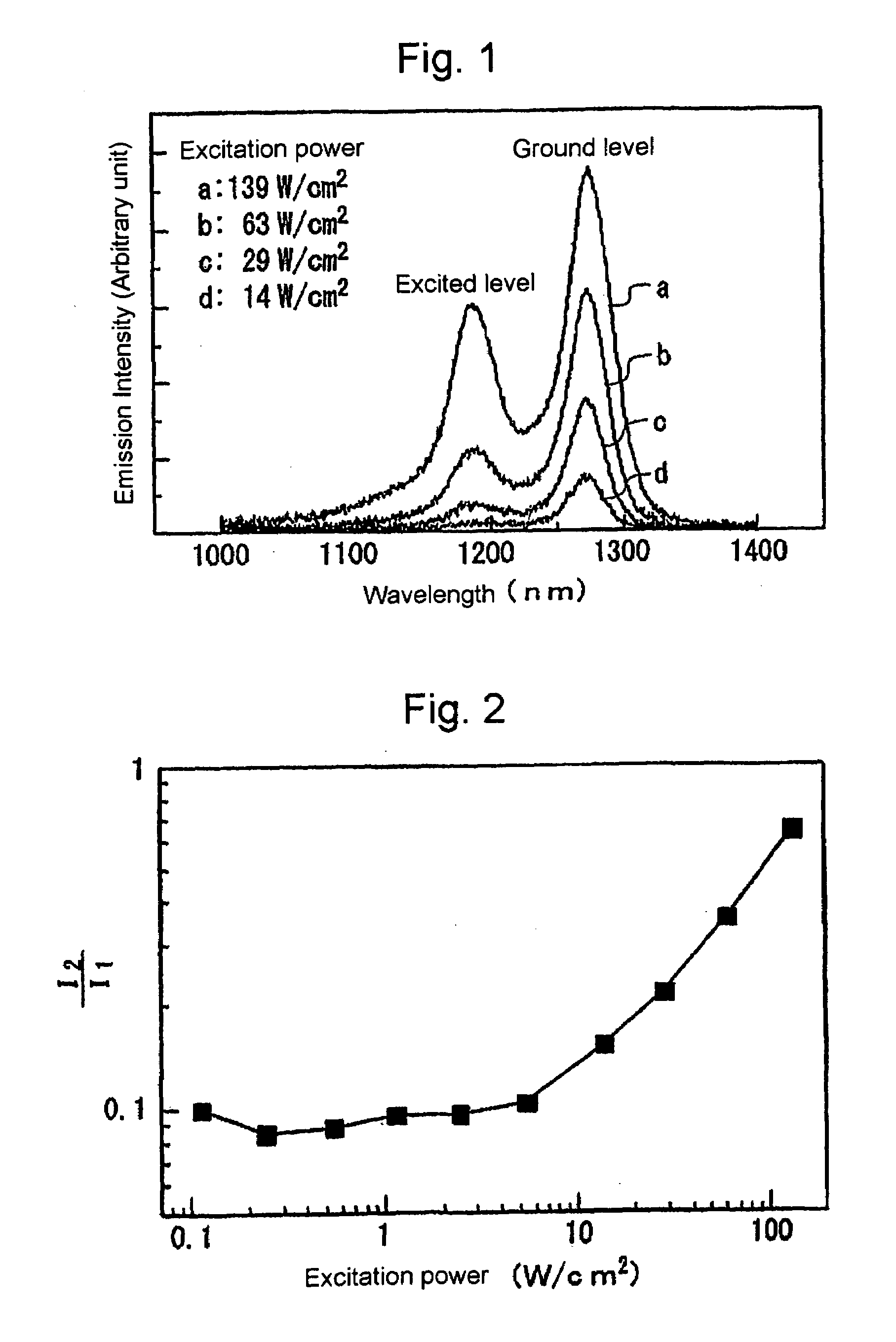
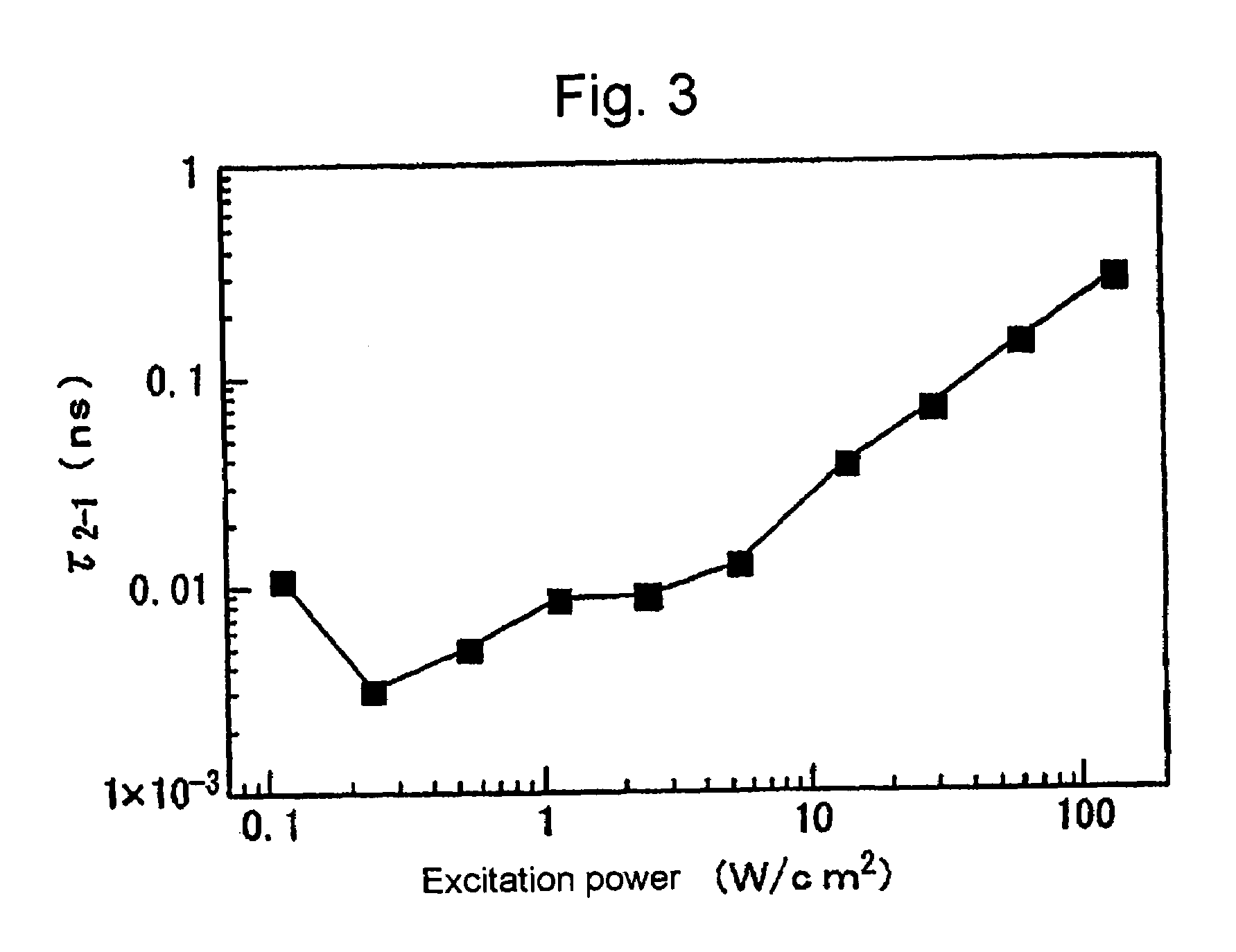
[0089]FIG. 8 shows the construction of a first example of a quantum dot laser in which the semiconductor quantum dot device of the present invention has been applied.

[0090]The quantum dot laser shown in FIG. 8 was fabricated by the following procedure which used an MBE (Molecular Beam Epitaxy) apparatus.

[0091]First, n-type AlGaAs cladding layer 22 (aluminum composition of 0.3, thickness of 3 μm, and carrier concentration of 1×1018 cm−3), undoped GaAs optical confinement layer 23 (thickness of 0.15 μm), and undoped GaAs barrier layer 24 (thickness of 20 nm) are successively grown on n-type GaAs substrate 21.

[0092]The temperature of GaAs substrate 21 is next set to 490° C. and InAs is grown on undoped GaAs barrier layer 24 while regulating the amount such that the InAs having a thickness equivalent to a three-atom layer is grown. At this time, undoped InAs quantum well layer (referred to as a “wefting layer”) 25 is first formed to a thickness equivalent to one- or two-atom layer, foll...

second example

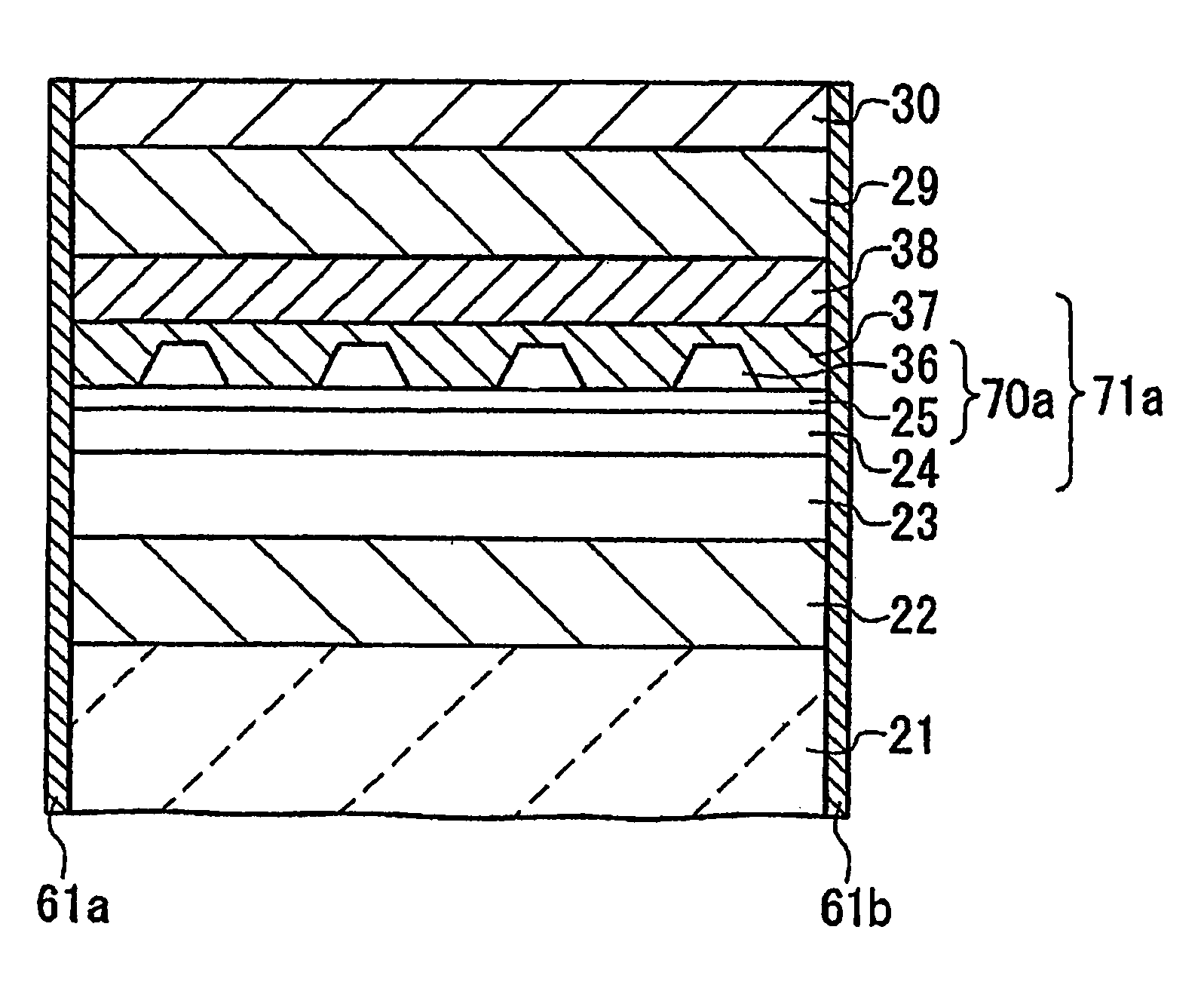
[0101]FIG. 9 shows the construction of the second example of a quantum dot laser in which the semiconductor quantum dot device of the present invention is applied.

[0102]The quantum dot laser of the second example is a construction in which undoped InAs quantum dots 36, p-type GaAs barrier layer 37, and p-type GaAs optical confinement layer 38 are formed in place of p-type InAs quantum dots 26, undoped GaAs barrier layer 27, and undoped GaAs optical confinement layer 28, respectively, in the first example. The construction is otherwise identical to that of the semiconductor laser of the first example, and constituent elements which are identical to elements in the first example are therefore identified by the same reference numbers and redundant detailed explanation is here omitted.

[0103]The quantum dot laser of the second example was fabricated by the following process using an MBE apparatus as in the first example.

[0104]As in the first example, n-type AlGaAs cladding layer 22, undo...


PUM


Abstract

A p-type semiconductor barrier layer is provided in the vicinity of undoped quantum dots, and holes in the p-type semiconductor barrier layer are injected in advance in the ground level of the valence band of the quantum dots. Lowering the threshold electron density of conduction electrons in the ground level of the conduction band of quantum dots in this way accelerates the relaxation process of electrons from an excited level to the ground level in the conduction band.

Description

TECHNICAL FIELD[0001]The present invention relates to electronic devices such as field effect transistors and single-electron elements as well as to semiconductor optical devices such as semiconductor lasers, semiconductor amplifiers, semiconductor optical switches, wavelength conversion elements, and optical memories which are used in, for example, optical communication and optical interconnections; and more particularly to a semiconductor quantum dot device which is provided with quantum dots.BACKGROUND ART[0002]Quantum dots can be called boxes of quantized potential on the hyperfine scale in which carriers (conduction electrons and holes) are confined in three dimensions. The density of the state function of carriers in a quantum dot is broken up according to a delta function, and the injected carriers are concentrated in these discrete energy levels. As a result, light which is emitted when the conduction electrons and holes recombine in the interior of quantum dots is of high o...

Claims


Application Information

Patent Timeline
Patent Type & Authority Patents(United States)
IPC IPC(8): H01L29/06H01S5/12H01S5/34H01S5/343
CPCB82Y20/00H01S5/341H01S5/3412H01S5/1228
Inventor SAITO, HIDEAKI
Owner NEC CORP
Why Eureka
Try Eureka