Reliability improvement of SiOC etch with trimethylsilane gas passivation in Cu damascene interconnects

a technology of trimethylsilane and interconnects, which is applied in the direction of semiconductor devices, semiconductor/solid-state device details, electrical apparatus, etc., can solve the problems of poor wafer to wafer reliability control, defeat the purpose of deposited low k dielectric layers, and increase the cost of etching, so as to reduce leakage current

Inactive Publication Date: 2007-03-20
TAIWAN SEMICON MFG CO LTD
View PDF6 Cites 25 Cited by
  • Summary
  • Abstract
  • Description
  • Claims
  • Application Information

AI Technical Summary

Benefits of technology

[0012]An objective of the present invention is to reduce leakage current in a semiconductor device and particularly in metal layers that are fabricated by a damascene process.
[0013]A further objective of the present invention is to enhance throughput in a damascene method while lowering the cost of the process.
[0014]A still further objective of the present invention is to improve via Rc stability in a semiconductor device by employing a SiCOH barrier / etch stop layer in a damascene method.
[0015]Yet another objective of the present invention is to provide improved wafer to wafer and within wafer reliability control by minimizing process instability from etch stop layer thickness variations.
[0016]Still another objective of the present invention is to provide an improved method of forming an etch stop layer in a damascene process that is compatible with existing tools and processes.

Problems solved by technology

A porous structure will allow moisture uptake which increases the dielectric constant and defeats the purpose of depositing a low k dielectric layer.
Furthermore, large process instability is observed due to SiC thickness variations that result in poor wafer to wafer and within wafer reliability control.
In some applications, however, adhesion of the SiCOH dielectric layer to the substrate may suffer because of a lack of a barrier layer that functions as a glue layer.

Method used


Image

  • Reliability improvement of SiOC etch with trimethylsilane gas passivation in Cu damascene interconnects
  • Reliability improvement of SiOC etch with trimethylsilane gas passivation in Cu damascene interconnects
  • Reliability improvement of SiOC etch with trimethylsilane gas passivation in Cu damascene interconnects

Examples


second embodiment

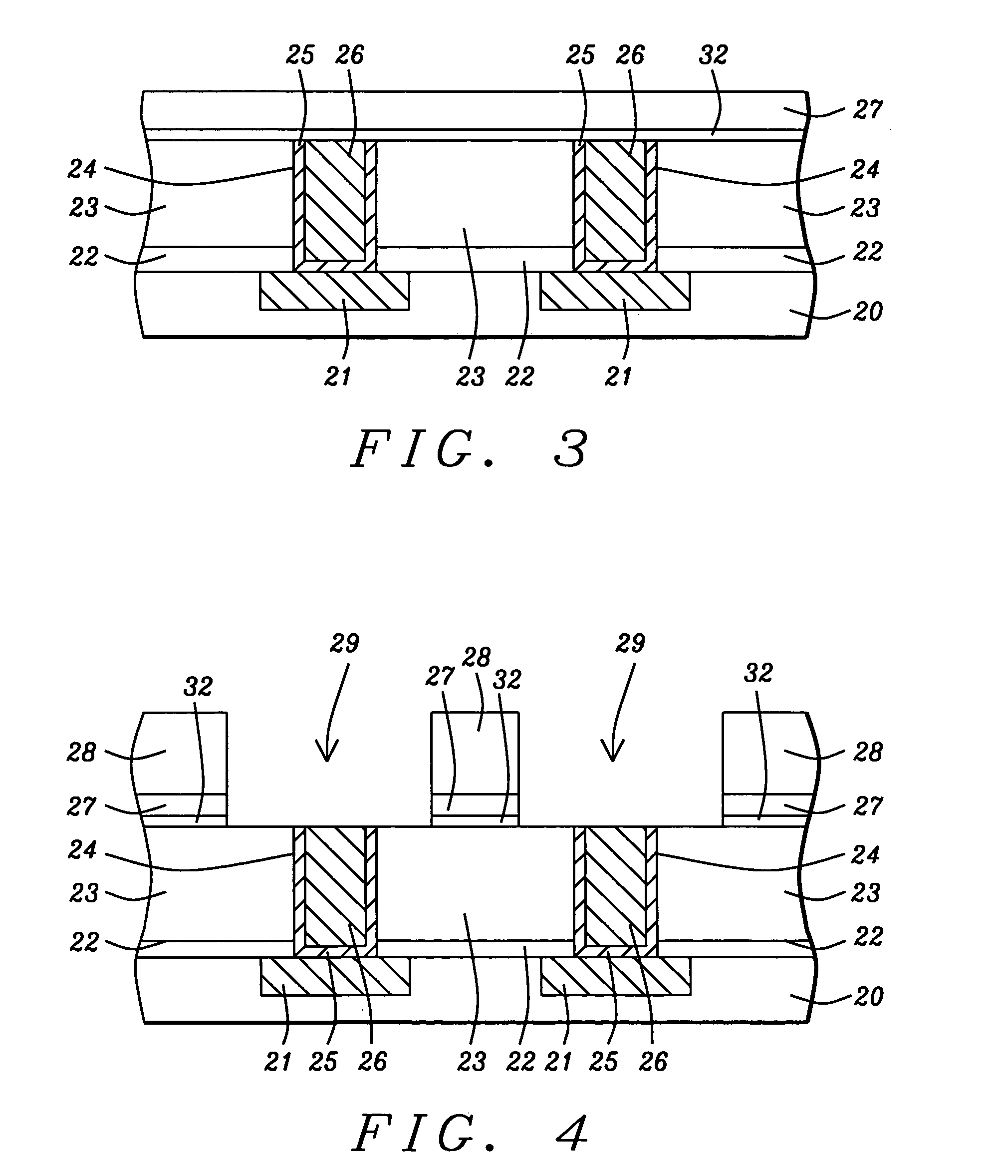
[0036]Those skilled in the art will appreciate that a SiCOH etch stop layer deposited according to the present invention could also be formed on metal lines in a gap fill process (not shown). For example, a SiCOH etch stop layer formed according to the first or second embodiment may be deposited as a conformal layer on the top surfaces and sidewalls of etched metal lines and then a thicker dielectric layer such as fluorosilicate glass may be deposited on the SiCOH etch stop layer to fill the gaps between the metal lines as appreciated by those skilled in the art.

first embodiment

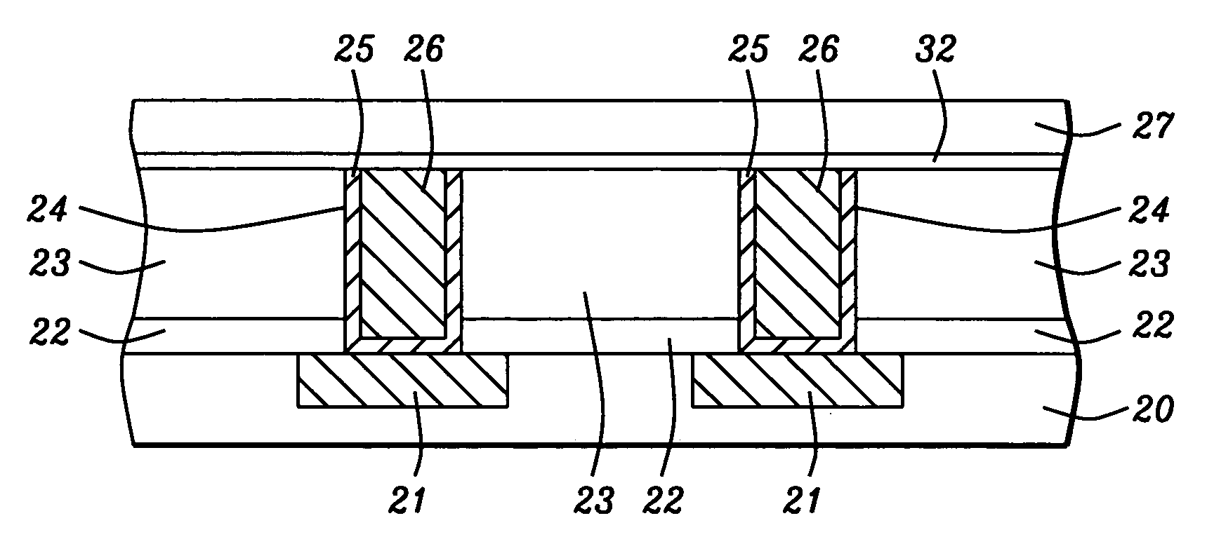
[0037]The drawings are provided by way of example and are not intended to limit the scope of the invention. A first embodiment is described in FIGS. 3–10. Referring to FIG. 3, a substrate 20 is provided that is typically monocrystalline silicon but also may be based on silicon-germanium, gallium-arsenide, or silicon-on-insulator technology. Substrate 20 usually contains active and passive devices (not shown). In one embodiment, the substrate 20 is also comprised of a conductive layer 21 that may be W, Al, Al / Cu or copper. The conductive layer 21 typically includes a plurality of metal lines and each metal line may be bounded on the sides and bottom by a diffusion barrier layer (not shown). A planarization method such as a chemical mechanical polish step is performed so that the conductive layer 21 is coplanar with the top surface of the substrate 20.

[0038]A stack of dielectric layers that include a first etch stop layer 22 and a first low k dielectric layer 23 are sequentially depos...


PUM

PropertyMeasurementUnit
compressive stressaaaaaaaaaa
thicknessaaaaaaaaaa
thicknessaaaaaaaaaa

Abstract

A method of forming a SiCOH etch stop layer in a copper damascene process is described. A substrate with an exposed metal layer is treated with H2 or NH3 plasma to remove metal oxides. Trimethylsilane is flowed into a chamber with no RF power at about 350° C. to form at least a monolayer on the exposed metal layer. The SiCOH layer is formed by a PECVD process including trimethylsilane and CO2 source gases. Optionally, a composite SiCOH layer comprised of a low compressive stress layer on a high compressive stress layer is formed on the substrate. A conventional damascene sequence is then used to form a second metal layer on the exposed metal layer. Via Rc stability is improved and a lower leakage current is achieved with the trimethylsilane passivation layer. A composite SiCOH etch stop layer provides improved stress migration resistance compared to a single low stress SiCOH layer.

Description

FIELD OF THE INVENTION[0001]The invention relates to the field of fabricating integrated circuits and other electronic devices and in particular to a lower cost method of making a copper interconnect with improved reliability and less leakage current.BACKGROUND OF THE INVENTION[0002]The manufacture of an integrated circuit in a semiconductor device involves the formation of a metal layer which is overlaid on another conductive layer to form a wiring pattern. This process is usually repeated several times to produce a stack of metal layers. Metal interconnects which form horizontal and vertical electrical pathways in the device are separated by dielectric layers to prevent crosstalk between the metal wiring that can degrade device performance by slowing circuit speed.[0003]A popular method of making an interconnect structure is a damascene process in which an opening is formed in a stack of dielectric layers. In a single damascene scheme, the opening which is a via, contact hole, or ...

Claims


Application Information

Patent Timeline
Patent Type & Authority Patents(United States)
IPC IPC(8): H01L23/48H01L21/306H01L21/314H01L21/316H01L21/4763H01L21/768
CPCH01L21/02126H01L21/02211H01L21/02274H01L21/02304H01L21/02315H01L21/76832H01L21/31633H01L21/76829H01L21/02046H01L21/3145H01L21/3148H01L21/76807H01L21/3144
Inventor WU, ZHEN-CHENGCHEN, BI-TROUGCHANG, WENGJANG, SYUN-MINGLIN, SU-HORNG
Owner TAIWAN SEMICON MFG CO LTD
Why Eureka
Try Eureka