
Parallel oversampling algorithmic A/D converter and method of using the same

Active Publication Date: 2007-10-30
TOYOTA JIDOSHA KK
View PDF17 Cites 68 Cited by
  • Summary
  • Abstract
  • Description
  • Claims
  • Application Information

AI Technical Summary

Benefits of technology

[0022]The present invention has been made to solve the problems with the above-described conventional A / D converter and the method therefore. That is, an object of the present invention is to provide an A / D converter of a new system which performs both of a high precision and a high speed at the same time and is low in the costs, and a method of conducting the A / D conversion.
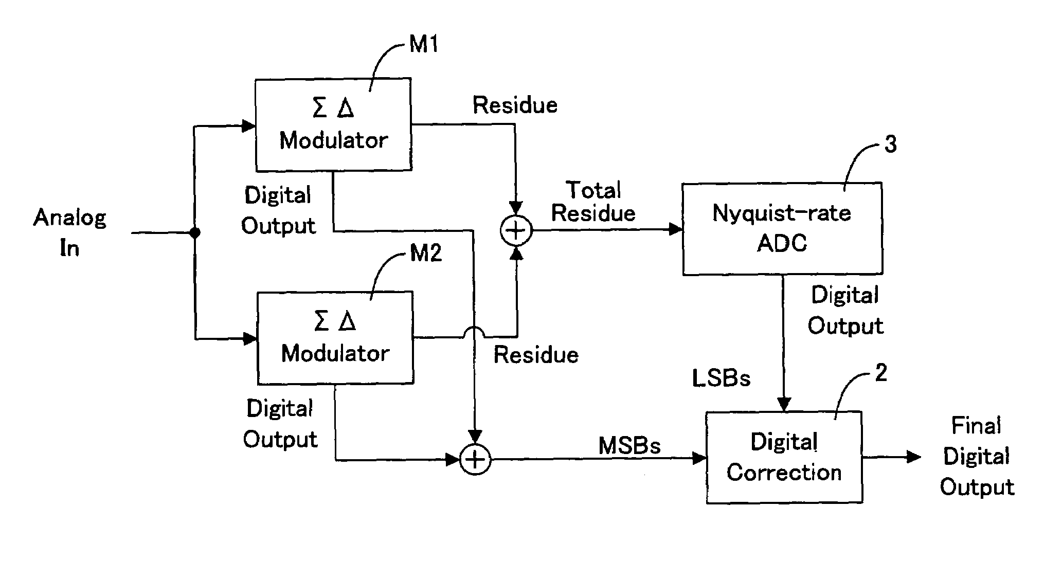
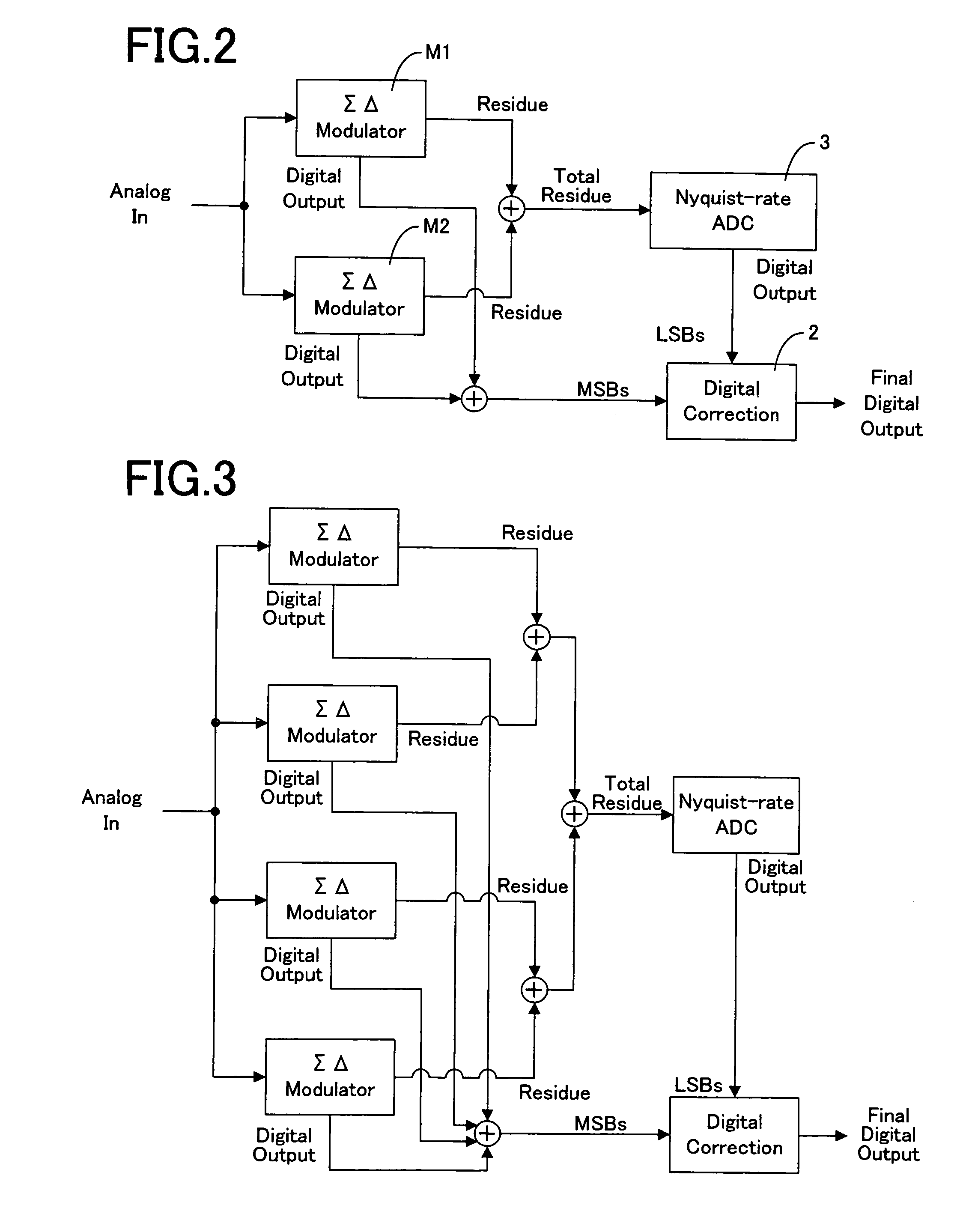
[0025]That is, in the present invention, the parallel oversampling of the analog input signal is conducted by the plural sigma-delta modulators. Then, the quantized values in the respective sigma-delta modulators are added together to obtain MSBs. In addition, the residue values of the integrators after quantization are added together, and its result is subjected to digital conversion to thereby obtain LSBs. The composition of the MSBs and the LSBs, which is obtained as described above, is a digital conversion value of the analog input signal. Both of the parallel oversampling and the addition of the residue values are ratio independent operations. For that reason, an accurate value that is not affected by the matching error (ratio precision) of the capacitor is obtained. Also, since the input signal can be simply processed, a parasitic capacitance at an input side can be reduced. For that reason, the present invention is capable of conducting arithmetic operation without degrading the linearity of the sigma-delta modulator and suits the arithmetic operation with high speed and high precision.
[0026]According to the present invention, there are provided the A / D converter of the new system which performs both of the high precision and the high speed at the same time and is low in the costs, and a method therefore. These and other objects and many of the attendant advantages of the invention will be readily appreciated as the same becomes better understood by reference to the following detailed description when considered in connection with the accompanying drawings.

Problems solved by technology

However, the above-mentioned conventional algorithmic A / D converter suffers from the following problems.
First, a sampling capacitor large in capacitance is required.
In fact, the noise of the operational amplifier is added to the capacitor noise.
That the sampling capacitor is large means that the operating speed cannot be ensured unless the driving performance of the operational amplifier is increased in proportion to the capacitor capacitance.
For that reason, the sizes of the respective elements that configure the operational amplifier and a bias current must be increased with the results that the chip area becomes large and a current consumption becomes excessive.
For that reason, kickback noise is generated at the time of switching.
This fact means that driving impedance at a fore part of the A / D converter is large, and an influence of the kickback noise on the circuit is large, and an error is large.
This will be a problem particularly in the high-precision A / D converter.
On the other hand, in order to reduce the impedance of a signal source, an additional amplifier must be added, which is disadvantageous in the circuit costs and the power consumption.
Second, there arises a problem on the matching precision in the capacitor capacitance within a semiconductor integrated circuit.
This is because the capacitance of the respective capacitors within the same chip is slightly uneven due to the manufacturing variation.
The algorithm of that type is complicated and large in the number of arithmetic operation steps, and long in conversion time.
This problem can be eliminated by trimming the capacitor, but the trimming causes an increase in the costs.
Third, a high-gain operational amplifier is required.
However, an actual problem resides in that it is difficult to design the operational amplifier that is too high in the gain, wide in the output range, and high in the operating speed.
This difficulty is especially serious in the case where a supply voltage is low and in the deep sub-micron process.
However, this leads to disadvantages such as an increase in the chip area and a degradation in a response speed.
It is needless to say that this structure is disadvantageous in the costs.
However, the ΣΔ modulator requires about several tens to several hundreds as the oversampling ratio, and does not suit the high speed processing.
Because the fine CMOS cannot be used, for example, in an in-vehicle 5 V power integrated circuit, the chip area of the large-scale logic circuit becomes remarkably large.
Even though the processing of the digital decimation filter can be realized by a microcomputer, a load of the microcomputer is significantly large in order to obtain the necessary processing speed, so the realization of such microcomputer is not easy.
However, in fact, the modulator that is high in the conversion speed and the response input frequency could not be realized.
First, both of the high precision and the high speed cannot be performed at the same time.
This is because the large number of times of sampling is required.
However, this conflicts with increasing the number of times of sampling.
To achieve this, the sizes of the structural elements must be increased, and the power consumption becomes high.
This conflicts with the requirements of the high speed and the small chip area.
Also, the kickback noise at the time of turning on / off the capacitor cannot be ignored.
Notwithstanding, this prevents both of the high speed and the high precision from being performed at the same time.
This is because an error in the operational amplifier finite gain of the first-order ΣΔ modulator is in proportion to an output voltage divided by the gain.
However, as described above, it is difficult to design the operational amplifier that is high in the gain and wide in the output range.
In particular, in the case where the supply voltage is low and the fine CMOS process is used, the sufficient gain cannot be obtained by provision of only the single-stage operational amplifier and the gain booster.
In any case, it is difficult to prevent the chip area or the power consumption from increasing.

Method used


Image

  • Parallel oversampling algorithmic A/D converter and method of using the same
  • Parallel oversampling algorithmic A/D converter and method of using the same
  • Parallel oversampling algorithmic A/D converter and method of using the same

Examples


Embodiment Construction

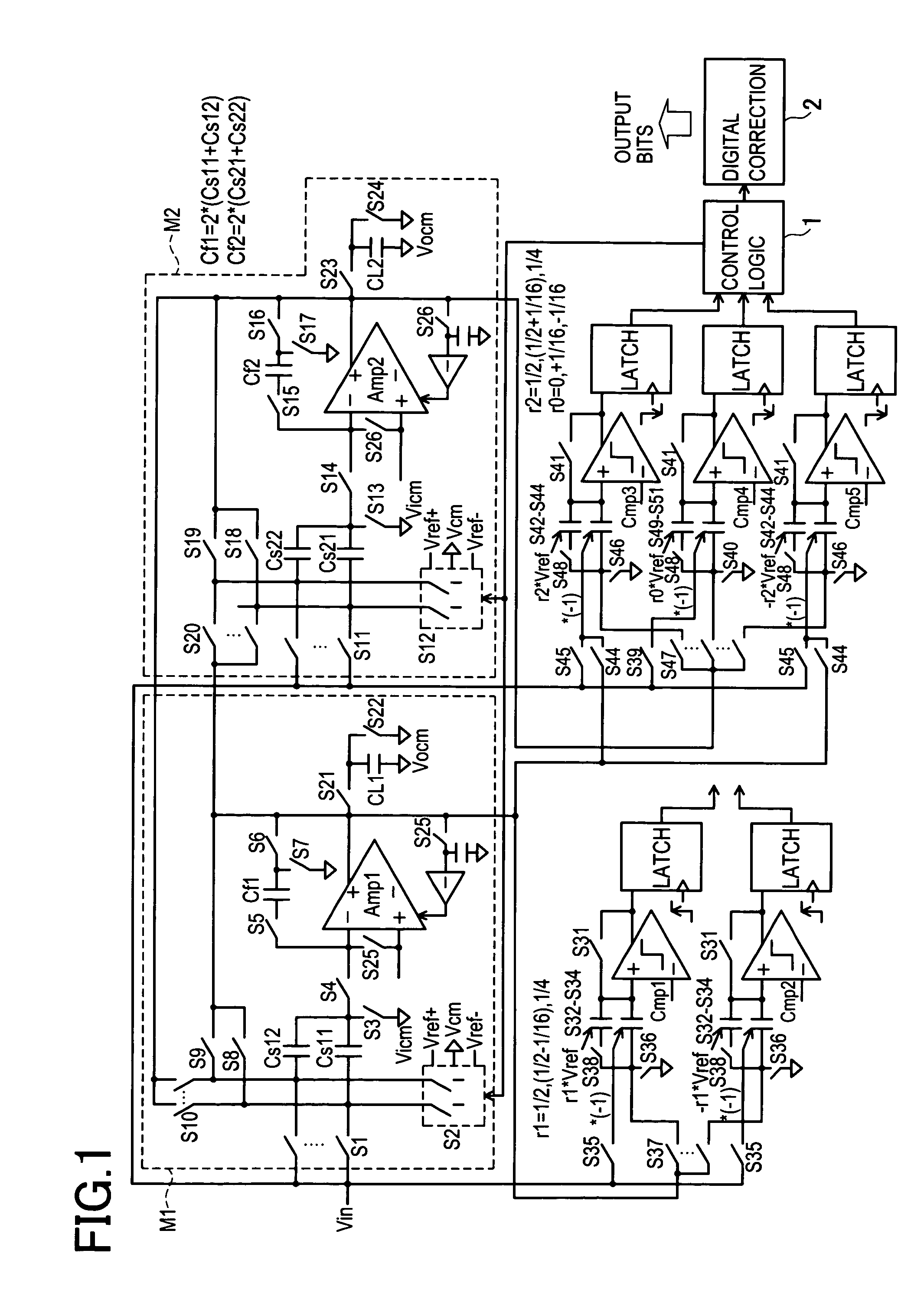
[0069]Now, a description will be given of preferred embodiments of the present invention with reference to the accompanying drawings. A circuit diagram of an A / D converter according to this embodiment is shown in FIG. 1. In the circuit diagram, one group centered on an operational amplifier Amp1 is the first ΣΔ modulator M1, and one group centered on an operational amplifier Amp2 is the second ΣΔ modulator M2. In the case of fully differential type, this circuit diagram shows only one side of the real circuit for simplicity. An analog input signal Vin is input into both of those ΣΔ modulators. In each of those ΣΔ modulators, an integrator is made up of an amplifier and capacitors which are arranged in parallel (Amp1 and Cf1, Amp2 and Cf2). A group centered on a comparator and a latch at a lower side of FIG. 1 is an operation section.

[0070]The ΣΔ modulators will be described in more detail. In the ΣΔ modulator M1, two capacitors Cs11 and Cs12 (hereinafter referred to as “sampling cap...


PUM


Abstract

Each of plural sigma-delta modulators having a sampling capacitor, an integrator, and a quantizer are connected to each other in parallel. Each of the sigma-delta modulators conducts parallel oversampling in which an analog input signal is sampled by a sampling capacitor, and the sampling result is quantized by the integrator and the quantizer. Then, the quantized values of the sigma-delta modulators are added to obtain MSBs, the residue values of the integrators after quantizing in the respective sigma-delta modulators are added, and the addition result of the residue values is converted analog-to-digital to obtain LSBs.

Description

BACKGROUND OF THE INVENTION[0001]1. Field of the Invention[0002]The present invention relates to an Analog-to-Digital (A / D) converter configured as a semiconductor integrated circuit, and a method for the A / D converter. More particularly, the present invention relates to a parallel oversampling algorithmic A / D converter and a method therefore. For example, the present invention is preferable to an A / D converter and a method therefore with a middle-to-high precision (12 to 16 bits) and a middle-to-high speed (100 k to 10 MHz) which is equipped in an in-vehicle sensor or a control microcomputer.[0003]2. Description of Related Art[0004]Up to now, an algorithmic A / D converter for a middle precision and middle speed has been employed. The algorithmic A / D converter is also called “cyclic ADC type”. Simply stated, an analog input signal is repeatedly subjected to comparison by a comparator and multiply-by-two operation, to thereby generate digital data in the order from MSB. The multiply-b...

Claims


Application Information

Patent Timeline
IPC IPC(8): H03M1/12
CPCH03M3/35H03M3/326H03M3/46H03M1/14H03M3/02
Inventor WATANABE, HIKARU
Owner TOYOTA JIDOSHA KK
Learn More