Preview mode low resolution output system and method
Inactive Publication Date: 2007-12-04
CIRRUS LOGIC INC
View PDF23 Cites 19 Cited by
Summary
Abstract
Description
Claims
Application Information
AI Technical Summary
This helps you quickly interpret patents by identifying the three key elements:
Problems solved by technology
Method used
Benefits of technology
[0007]According to one embodiment of the present invention, a processing system for an imager device includes a camera system for producing a desired imager signal which operates in a reduced power or preview mode. Such a system according to the present invention includes a correlated double sample (CDS) circuit for receiving data from a selected imager, a multi-mode (selectably high or low current) variable gain amplifier (VGA), a low power mode analog-to-digital converter (ADC) having a selectable narrow bit-width output and coupled to said CDS circuit. The low power mode enables production of an ADC output signal of selectable higher or lower resolution. The processing system according to the present invention includes a gain adjust block (GAB) coupled to the ADC, a black level adjustment circuit including a predetermined clamp setting, a compander circuit coupled to said GAB for further reducing the output bit-width, a multiplexer permitting selection of output signals of selected bit-width, and a phase-lock-loop (PLL) for controlling a multi-sync timing generator including an analog clock generator (ACG). According to the present invention, the compander bit-width reduction compresses the output so a smaller bit-width signal can retain the same dynamic range as a larger bit-width signal, while the ADC output bi
Problems solved by technology
To practically capture a CCD image, the data read-out time from the CCD is very limited.
Such extended functionality comes at a price in terms of electronic complexity and power consumption.
This can dissipate a large amount of powe
Method used
Image
Click on the blue label to locate the original text in one second.
Reading with bidirectional positioning of images and text.
Examples
Embodiment Construction
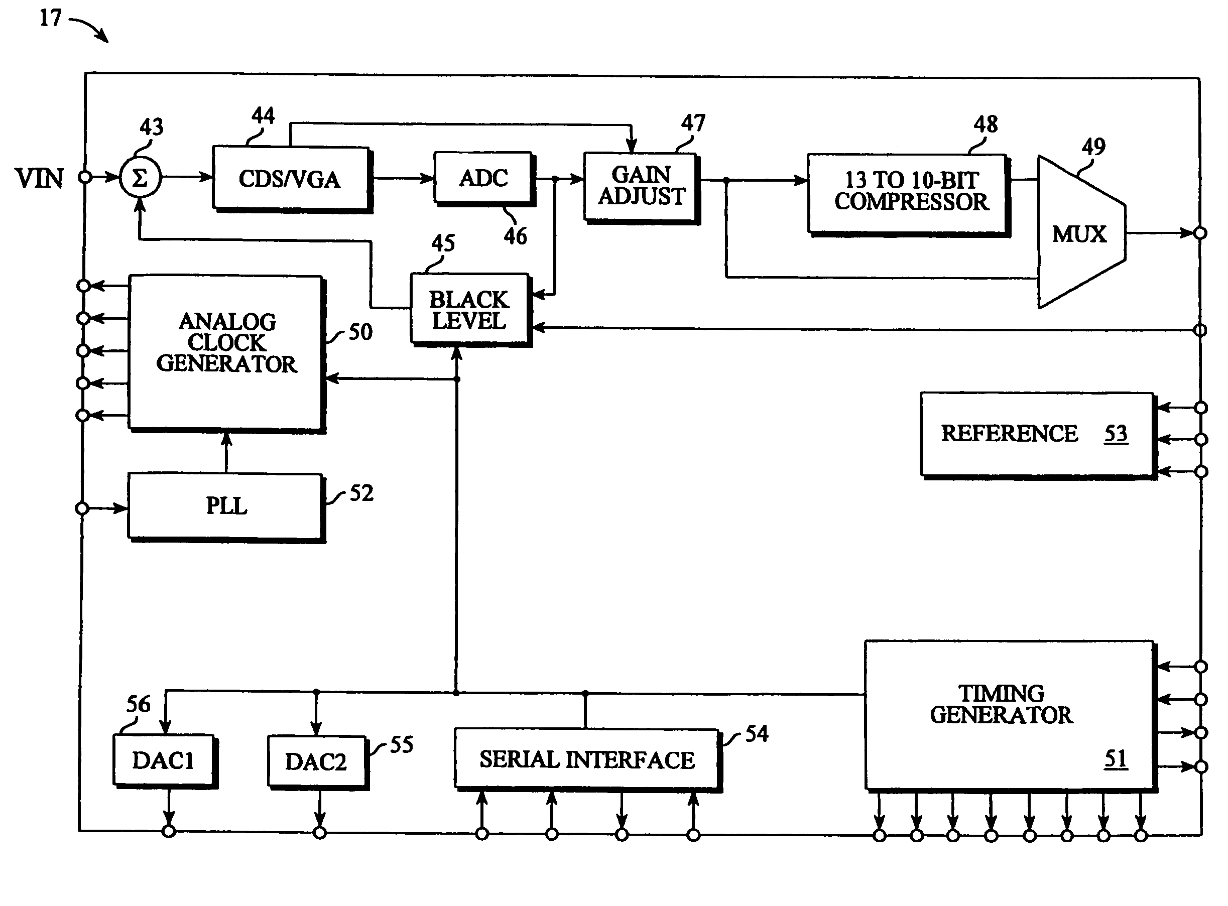
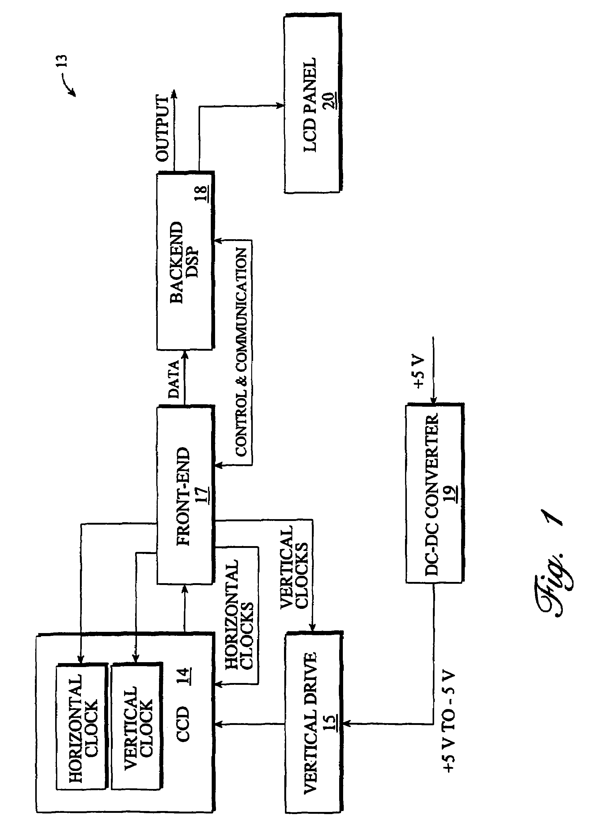
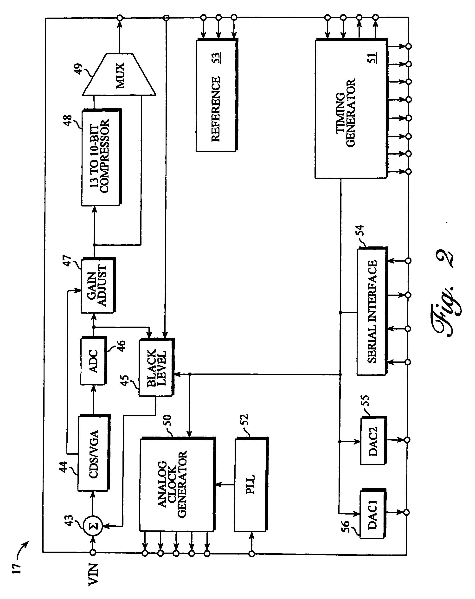
[0018]Referring now to FIG. 1, there is shown a block diagram of a camera system 13, according to the present invention. As shown in FIG. 1, camera system 13 according to the present invention includes the following integrated circuit (IC) components, according to one embodiment of the present invention: a CCD array sensor 14, a vertical driver circuit 15, first and second signal processing subsystems (SPS) 17 and 18 (i.e., a front-end and a back-end subsystem), a DC-to-DC converter 19, and a display system such as for example without limitation a liquid crystal display (LCD) panel 20. The LCD panel 20 is connected to second SPS 18 for receipt of a digital signal input. First SPS 17 is an analog signal processing (ASP) front-end (AFE) system which receives and processes video samples from the CCD array sensor 14 and generates timing clocks and pulses required by the CCD array sensor 14, and vertical driver circuit 15. The vertical driver circuit 15 generates high voltage vertical sh...
PUM
Abstract
A processing system for a charge coupled device (CCD) or CMOS imaging system includes a correlated double sample (CDS) circuit for receiving data from an imager, a variable gain amplifier (VGA) having amplifiers of selectable current level to enable reduced data resolution in a preview display, a low power mode analog-to-digital converter (ADC) having a selectable narrow bit-width output and coupled to said VGA circuit, and a gain circuit coupled to said ADC. The single chip low-power analog front end produces digitized CCD data in either 13-bit, 12-bit or 10-bit formats at a first current level and 9-bit, 8-bit, or 6-bit formats at a second current level. The VGA amplifier includes symmetrical subcircuits which are independently actuable to enable full or reduced data resolution levels respectively for still image capture operation and video previewing on a separate preview screen.
Description
CROSS REFERENCE TO RELATED APPLICATIONS[0001]This application is a continuation application of U.S. patent application Ser. No. 09 / 282,524, filed Mar. 31, 1999, now U.S. Pat. No. 6,686,957 entitled “Preview Mode Low Resolution Output System and Method” having inventors Sandra M. Johnson, Douglas R. Holberg, and Nadi R. Itani and is related to patent application Ser. Nos. 09 / 283,098; 09 / 283,112; 09 / 282,515; 09 / 283,779; 09 / 282,523, respectively entitled “Phase Locked Loop Circuits, Systems, and Methods” having inventors Douglas R. Holberg and Sandra Marie Johnson; “CCD Imager Analog Processor Systems and Methods” having inventors Douglas R. Holberg, Sandra Marie Johnson, Nadi Rafik Itani, and Argos R. Cue; “Amplifier System with Reducable Power” having as inventor Nadi Rafik Itani; “Dynamic Range Extender Apparatus, System, and Method for Digital Image Receiver System” having inventors Sandra Marie Johnson and Nadi Rafik Itani, which has issued into U.S. Pat. No. 6,252,536 on Jun. 26,...
Claims
Application Information
Patent Timeline
Application Date:The date an application was filed.
Publication Date:The date a patent or application was officially published.
First Publication Date:The earliest publication date of a patent with the same application number.
Issue Date:Publication date of the patent grant document.
PCT Entry Date:The Entry date of PCT National Phase.
Estimated Expiry Date:The statutory expiry date of a patent right according to the Patent Law, and it is the longest term of protection that the patent right can achieve without the termination of the patent right due to other reasons(Term extension factor has been taken into account ).
Invalid Date:Actual expiry date is based on effective date or publication date of legal transaction data of invalid patent.