Group III nitride crystals usable as group III nitride substrate, method of manufacturing the same, and semiconductor device including the same

a technology of nitride crystals and substrates, applied in the direction of crystal growth process, natural mineral layered products, water-setting substance layered products, etc., can solve the problems of reduced dislocation density, insufficient quality of group iii nitride crystals obtained using conventional techniques, and complicated manufacturing processes. achieve the effect of high quality, useful and usable, and efficient manufacturing

Inactive Publication Date: 2007-12-18
PANASONIC CORP +1
View PDF24 Cites 10 Cited by
  • Summary
  • Abstract
  • Description
  • Claims
  • Application Information

AI Technical Summary

Benefits of technology

[0010]With such situations in mind, the present invention is intended to provide Group III nitride crystals that are of high quality, are manufactured efficiently

Problems solved by technology

Generally, crystals obtained by this method have a dislocation density of about 108 cm−2 to 109 cm−2 and thus the reduction in dislocation density has been an important issue for this method.
With this method, the dislocation density can be reduced to about 105 cm−2 to 106 cm−2, but the manufacturing process is complicated, which is another problem.
However, the quality of the Group

Method used


Image

  • Group III nitride crystals usable as group III nitride substrate, method of manufacturing the same, and semiconductor device including the same
  • Group III nitride crystals usable as group III nitride substrate, method of manufacturing the same, and semiconductor device including the same
  • Group III nitride crystals usable as group III nitride substrate, method of manufacturing the same, and semiconductor device including the same

Examples


embodiment 1

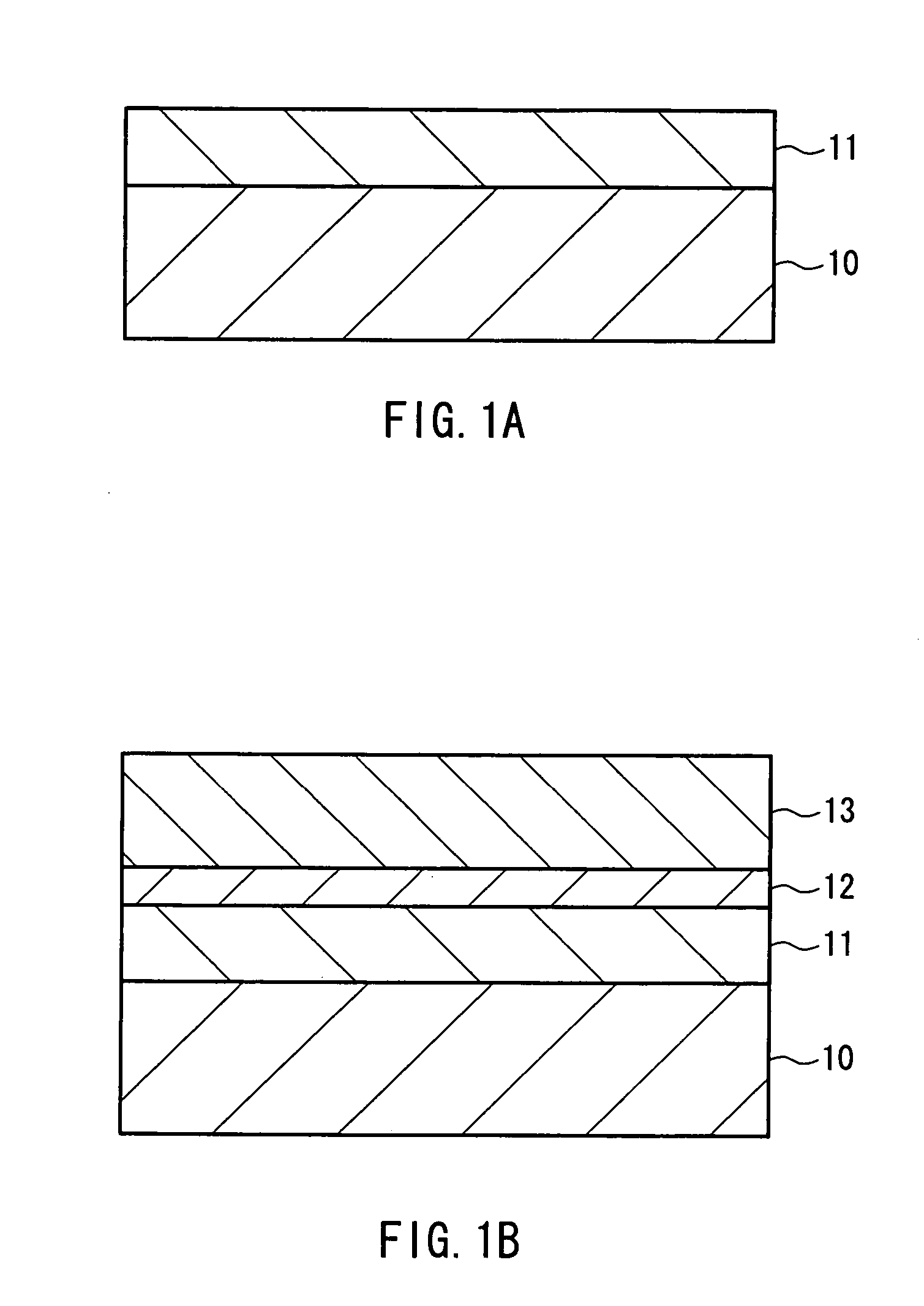
[0072]In this method, first, a first layer 11 is formed by a vapor growth method (step (i)). The first layer 11 is made of semiconductor crystals that are expressed by a composition formula of AlsGatIn1-s-tN (where 0≦s≦1, 0≦t≦1, and s+t≦1). As shown in FIG. 1A, the first layer 11 is formed on a substrate 10. Examples of the substrate 10 include a sapphire substrate (whose surface is, for example, a (0001) plane), a GaAs substrate (whose surface is, for example, a (111) plane), a Si substrate (whose surface is, for example, a (111) plane), and a SiC substrate (whose surface is, for example, a (0001) plane). The first layer 11 is a seed layer to serve as seed crystals. The first layer 11 is made of, for instance, GaN or AlsGa1-sN. Such a semiconductor layer can be formed by a vapor growth method such as a metalorganic chemical vapor deposition (MOCVD) method, a molecular beam epitaxy (MBE) method, or a hydride vapor phase epitaxy (HVPE) method. The thickness of the first layer 11 is n...

embodiment 2

[0085]A semiconductor device of the present invention is described in Embodiment 2. The semiconductor device of the present invention is one formed using the Group III nitride substrate described in Embodiment 1. That is, the semiconductor device of Embodiment 2 is formed using the Group III nitride crystal layer (for instance, a gallium nitride crystal layer) included in the Group III nitride substrate of Embodiment 1. The present invention is applied to any semiconductor devices that are formed using a Group III nitride substrate, for instance, laser diodes, light emitting diodes, and transistors. Specific examples of such semiconductor devices are described in the examples below.

[0086]The present invention is described further in detail using following examples. The following examples are described using GaN crystals as an example. However, Group III nitride crystals that are expressed by a composition formula of AlxGayIn1-x-yN (where 0≦x≦1, 0≦y≦1, and x+y≦1) such as AlxGa1-xN an...

example 1

[0087]In this example, the Group III nitride semiconductor substrate is produced as an example by the method described in Embodiment 1.

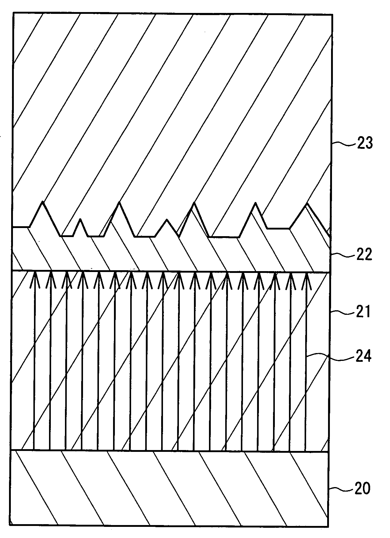
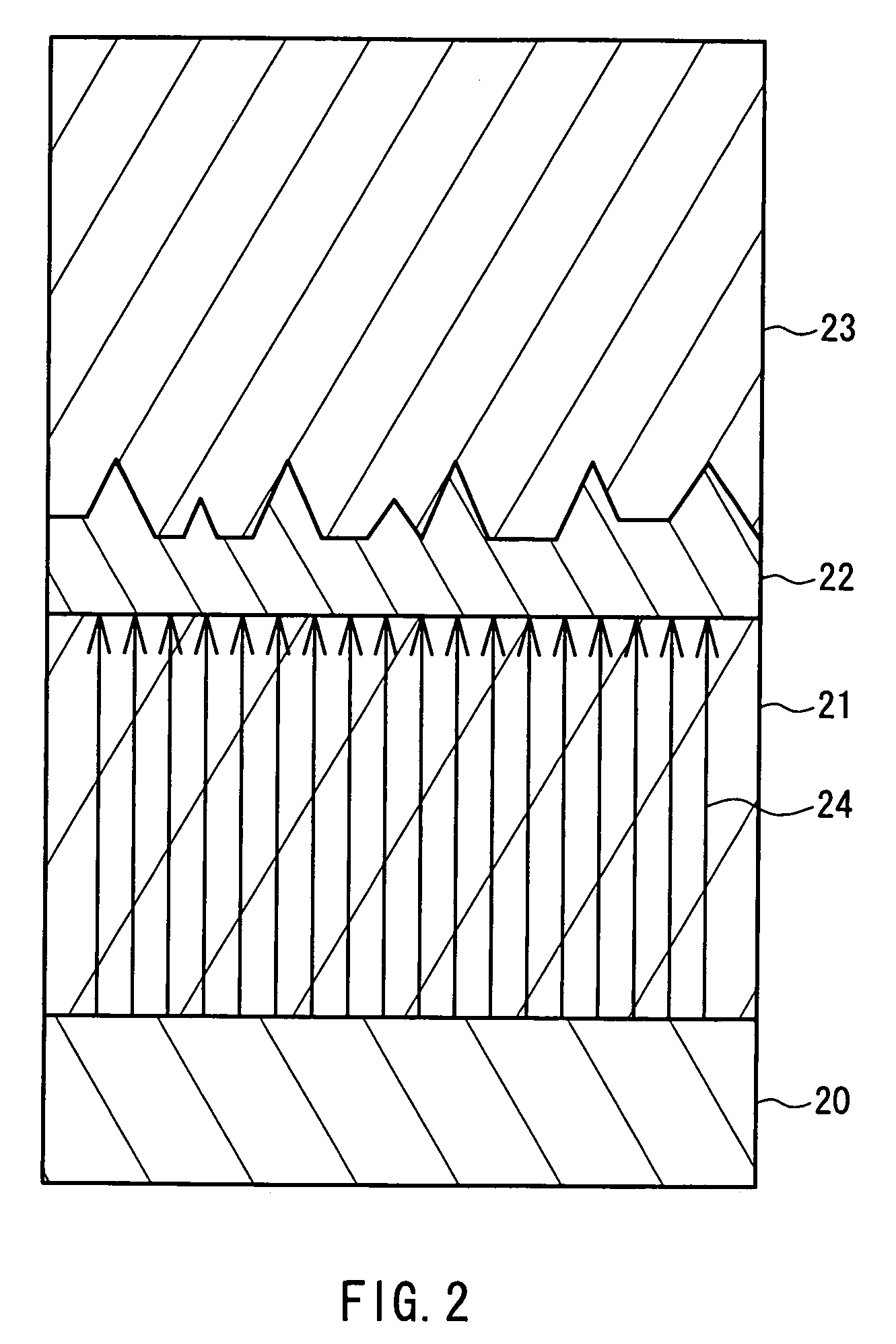
[0088]The Group III nitride substrate formed in this example has a configuration shown in FIG. 2. The Group III nitride substrate of the present example includes: a sapphire substrate 20 (corresponding to the substrate 10 shown in FIG. 1) made of sapphire (crystalline Al2O3); a seed layer 21 (the first layer) made of GaN; a high defect layer 22 (the second layer); and an LPE-GaN layer 23 (the third layer) formed by the liquid phase epitaxy method. The seed layer 21 is formed of a Group III nitride that is expressed by a composition formula of AlsGatIn1-s-tN (where 0≦s≦1, 0≦t≦1, and s+t≦1). In FIG. 2, the arrows 24 indicate edge dislocations.

[0089]The high defect layer 22 is formed in a melt containing alkali metal and at least one Group III element selected from gallium, aluminum, and indium. The present example is characterized in that the LPE-GaN l...


PUM

PropertyMeasurementUnit
Temperatureaaaaaaaaaa
Fractionaaaaaaaaaa

Abstract

The present invention provides a method of manufacturing Group III nitride crystals that are of high quality, are manufactured highly efficiently, and are useful and usable as a substrate that is used in semiconductor manufacturing processes. The method of manufacturing Group III nitride crystals includes: forming a first layer made of a semiconductor that is expressed by a composition formula of AlsGatIn1-s-tN (where 0≦s≦1, 0≦t≦1, and s+t≦1); forming a second layer by bringing the surface of the first layer into contact with a melt in an atmosphere including nitrogen, wherein the second layer includes greater defects in a crystal structure, such as a dislocation density for example, than those of the first layer, and the melt includes alkali metal and at least one Group III element selected from the group consisting of gallium, aluminum, and indium; and forming a third layer through crystal growth in the melt in an atmosphere including nitrogen, wherein the third layer is made of a semiconductor that is expressed by a composition formula of AluGavIn1-u-vN (where 0≦u≦1, 0≦v≦1, and u+v≦1), and the third layer has less defects in a crystal structure, such as a dislocation density for example, than those of the second layer.

Description

BACKGROUND OF THE INVENTION[0001]1. Field of the Invention[0002]The present invention relates generally to Group III nitride crystals that can be used as a Group III nitride substrate, a method of manufacturing the same, and a semiconductor device with the same.[0003]2. Related Background Art[0004]A Group III nitride compound semiconductor such as, for instance, gallium nitride (GaN) (hereinafter also referred to as a “Group III nitride semiconductor” or a “GaN-based semiconductor”) has been gaining attention as a material for semiconductor devices that emit blue or ultraviolet light. A laser diode (LD) that emits blue light is used for high-density optical disk devices or displays while a light emitting diode (LED) that emits blue light is used for displays, lighting, etc. It is expected to use an ultraviolet LD in the field of high technology such as, for example, biotechnology and an ultraviolet LED as, for example, an ultraviolet source for a fluorescent lamp.[0005]Substrates of...

Claims


Application Information

Patent Timeline
IPC IPC(8): B32B9/00B32B18/00C30B9/00H01L21/20H01L21/208H01L21/338H01L29/20H01L33/32
CPCH01L21/02389H01L21/0243H01L21/02458H01L33/32H01L21/0254H01L21/02625H01L29/66856H01L21/0237H01L21/02494H01L29/2003H01L21/02502
Inventor KITAOKA, YASUOMINEMOTO, HISASHIKIDOGUCHI, ISAOSASAKI, TAKATOMOMORI, YUSUKEKAWAMURA, FUMIOMORISHITA, MASANORI
Owner PANASONIC CORP
Why Eureka
Try Eureka