
Light emitting device and method of manufacturing a semiconductor device

a technology of light-emitting devices and semiconductor devices, which is applied in the direction of semiconductor devices, electrical equipment, transistors, etc., can solve the problems of increasing the probability of contact defects, low electric field effect mobility of tft using amorphous silicon, and inability to operate at the frequency required to process video signals

Inactive Publication Date: 2008-01-08
SEMICON ENERGY LAB CO LTD
View PDF86 Cites 53 Cited by
  • Summary
  • Abstract
  • Description
  • Claims
  • Application Information

AI Technical Summary

Benefits of technology

The present invention is about improving the characteristics of thin film transistors (TFTs) in a light emitting device using an organic compound as a light emitting layer. The invention aims to reduce the dispersion of the ON current (Ion) of TFTs and the OFF current, especially in the case of a TFT used as a switching element. The invention achieves this by arranging the channel length directions of the TFTs in a pixel portion in the same direction and aligning the scanning direction of laser light with the crystal growth direction. The invention also includes a driving circuit with multiple thin film transistors and a structure where the thin film transistors have a semiconductor film, insulating films, and electrodes. A constant voltage is applied to the first electrode to reduce fluctuation in Ion. Overall, the invention improves the performance and stability of the light emitting device.

Problems solved by technology

However, the TFT using amorphous silicon is low in electric field effect mobility, and cannot be operated at a frequency required to process the video signal.
An increase in the number of connecting terminal causes an increase in generating probability of a contact defect.
Further, the area (frame area) of a peripheral portion of a pixel section is increased and the compactness of a semiconductor device with and the design of an external appearance, as a display, are damaged.
However, even when the TFT is formed by using the polysilicon, its electrical characteristics are finally not equivalent to the characteristics of a MOS transistor formed in a monocrystal silicon substrate.
Further, the TFT using polysilicon has a problem that is dispersion is caused easily in its characteristics due to a defect formed in a boundary of a crystal grain.
Moreover, since the luminance of a pixel is determined by the ON current (Ion) of TFT which is electrically connected with an EL element and supplies current to the EL element without depending on the drive method, there is a problem dispersion is caused in luminance if ON current is not constant in case of displaying white on overall surface.

Method used


Image

  • Light emitting device and method of manufacturing a semiconductor device
  • Light emitting device and method of manufacturing a semiconductor device
  • Light emitting device and method of manufacturing a semiconductor device

Examples


embodiment mode 1

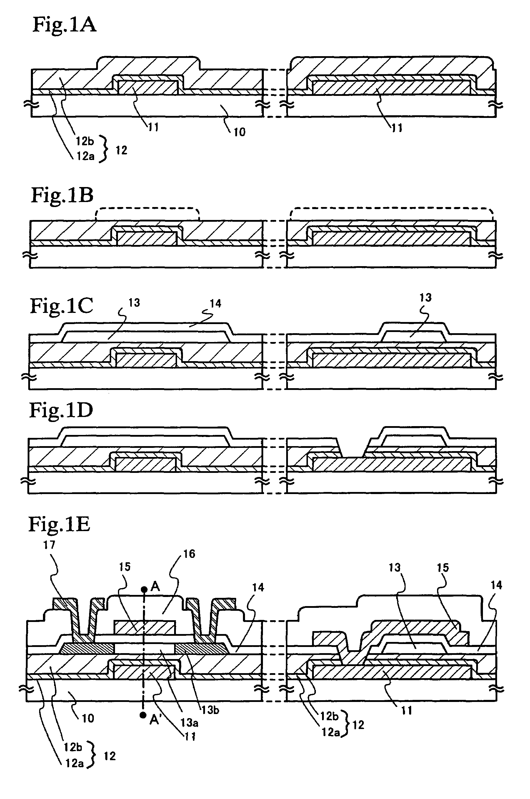
[0112]The following is a brief explanation on a typical procedure of manufacturing a TFT. The explanation is given with reference to FIGS. 1A to 1E.

[0113]In FIG. 1A, reference symbol 10 denotes a substrate which has an insulating surface, 11, a first electrode, and 12, a first insulating film.

[0114]First, a conductive film is formed on the substrate 10 and is patterned to form the first electrode 11 constituted of a metal or an alloy. Typically, the first electrode is formed from an alloy containing one or more kinds of elements selected from the group consisting of aluminum (Al), tungsten (W), molybdenum (Mo), tantalum (Ta), and titanium (Ti), or from an alloy containing silicon and one or more of the above elements. Alternatively, a laminate of several conductive films may be used for the first electrode. The first electrode 11 is 150 to 400 nm in thickness.

[0115]The first electrode 11 is a scanning line connected to a gate electrode that is formed later. The first electrode 11 ma...

embodiment mode 2

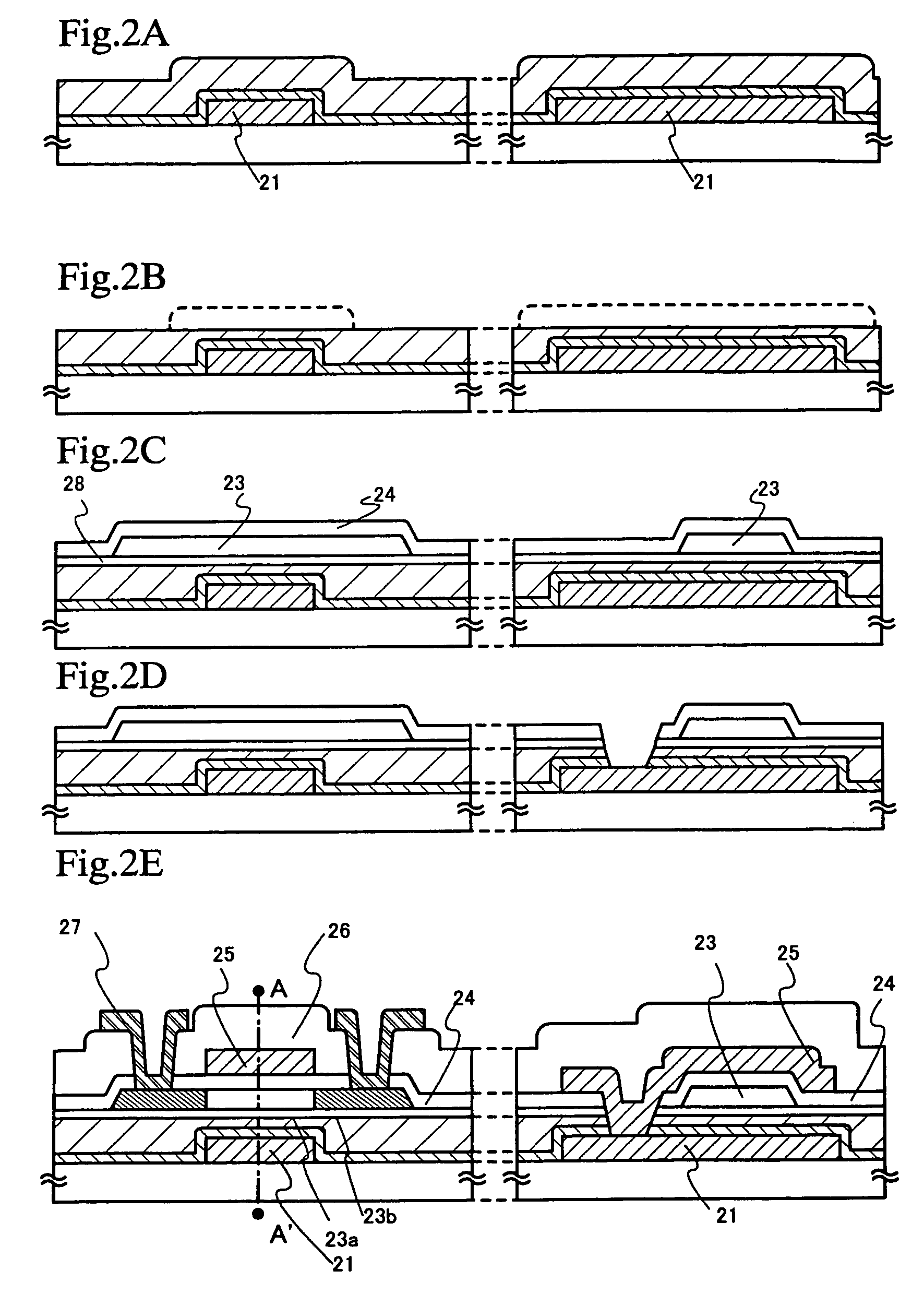
[0149]An example of manufacturing a TFT by a procedure different from the one in the above Embodiment Mode 1 is shown in FIGS. 2A to 2E.

[0150]FIG. 2A is identical with FIG. 1A. FIG. 2B is identical with FIG. 1B. This embodiment mode follows Embodiment Mode 1 until the state of FIG. 2B is reached.

[0151]After the state shown in FIG. 2B is reached, a second insulating film 28 is formed. An insulating film mainly containing silicon is used as the second insulating film 28. On the second insulating film 28, a semiconductor film 23 is formed following the procedure of Embodiment Mode 1 described above.

[0152]Next, the surface of the semiconductor film is washed with an etchant that contains fluoric acid to remove an oxide film or impurities. Then a third insulating film 24 mainly containing silicon is formed to serve as a gate insulating film. (FIG. 2C) Desirably, the surface washing and formation of third insulating film 24 are carried out continuously without exposing the substrate to th...

embodiment mode 3

[0158]An example of manufacturing a TFT by a procedure different from the one in the above Embodiment Mode 1 is shown in FIGS. 3A to 3E.

[0159]FIG. 3A is identical with FIG. 1A. FIG. 3B is identical with FIG. 1B. FIG. 3C is identical with FIG. 1C. This embodiment mode follows Embodiment Mode 1 until the state of FIG. 3C is reached.

[0160]After the state of FIG. 3C is reached, the surface of the second insulating film (gate insulating film) 34 is washed to form a second electrode 35 that serves as a gate electrode. Next, the semiconductor film is appropriately doped with an impurity element that gives a semiconductor the n type conductivity (such as P or As), here, phosphorus, to form impurity regions 33b. One of the impurity regions 33b serves as a source region and the other serves as a drain region. After doped with the impurity element, the semiconductor film is subjected to heat treatment, irradiation of intense light, or laser light irradiation in order to activate the impurity e...


PUM


Abstract

Semiconductor layers for serving as active layers of a plurality of thin film transistors in a pixel are arranged in the same direction and irradiated with laser light with the scanning direction matched to the channel length direction of the semiconductor layers. It is possible to coincide the crystal growth direction with the carrier moving direction, and high field effect mobility can be obtained. Also, semiconductor layers for serving as active layers of a plurality of thin film transistors in a driving circuit and in a CPU are arranged in the same direction, and are irradiated with laser light with the scanning direction matched to the channel length direction of the semiconductor layers.

Description

BACKGROUND OF THE INVENTION[0001]1. Field of the Invention[0002]The present invention relates to the manufacturing method of semiconductor device, in particular, present invention relates to a light emitting device comprising a light emitting element formed on a plastic substrate. The invention also relates to an EL module in which ICs including a controller, or the like, is mounted with an EL panel. Note that, in this specification, the light emitting device includes the EL panel and for the EL module. Electronic equipment using the light emitting device is also included in the present invention.[0003]Noted that in the present specification, the term “semiconductor device” generally indicates a device which is capable of functioning by utilizing semiconductor characteristics, and a light emitting device, an electro-optical device, a semiconductor circuit and an electronic device are all included in the semiconductor device.[0004]2. Description of the Related Art[0005]Recently, tech...

Claims


Application Information

Patent Timeline
Patent Type & Authority Patents(United States)
IPC IPC(8): H01L29/94H01L21/20H01L21/336H01L21/77H01L21/84H01L27/32H01L29/12H01L29/786H01L31/0328
CPCH01L21/2026H01L27/1285H01L27/1296H01L29/12H01L29/6675H01L29/78645H01L29/78648H01L27/3262H01L21/02683H01L21/02422H01L21/02502H01L21/02488H01L21/0242H01L21/02425H01L21/02686H01L21/02678H01L21/02491H01L21/02532H01L21/02381H01L21/02691H10K59/1213
Inventor YAMAZAKI, SHUNPEIKUWABARA, HIDEAKI
Owner SEMICON ENERGY LAB CO LTD
Learn More