Method for manufacturing a thin film transistor and method for manufacturing a semiconductor device

a thin film transistor and semiconductor technology, applied in transistors, chemical vapor deposition coatings, coatings, etc., can solve the problems of increasing the number of processes and costs, adverse effects on the device property of tft, and etching residues, so as to improve the mobility of the thin film transistor, improve the adverse effect of the crystal grain boundary, and achieve the effect of efficient gettering

Inactive Publication Date: 2008-03-25
SEMICON ENERGY LAB CO LTD
View PDF35 Cites 12 Cited by
  • Summary
  • Abstract
  • Description
  • Claims
  • Application Information

AI Technical Summary

Benefits of technology

[0028]According to the present invention, it is possible to form the crystalline semiconductor film having the crystal grain formed in order with which a thin film transistor having uniform electrical characteristic can be manufactured. In addition, the mobility of the thin film transistor can be improved when the channel-forming region is formed by conforming the direction of the crystal grain with the direction in which the current flows.
[0029]Moreover, the distance between the ridges, which is the distance between the crystal grains, is extremely short, which is almost equal to the wavelength of the laser light to be irradiated. For this reason, a plurality of crystal grains exist in the channel-forming region and therefore the adverse effect in the crystal grain boundary can be improved compared with the case in which the number of crystal grains is small.
[0030]In addition, the gettering step can be performed without forming an another gettering site by removing the ridge in which the metal element typified by Ni segregates. When the metal element further segregates, the metal element hardly exists outside the ridge and therefore the gettering can be performed efficiently.

Problems solved by technology

However, the metal element typified by Ni causes an adverse effect on the device property of TFT.
This gettering step, however, has disadvantages that the number of processes and the cost increase.
In addition, there is a problem of an etching residue when the gettering site is removed in the gettering step.

Method used


Image

  • Method for manufacturing a thin film transistor and method for manufacturing a semiconductor device
  • Method for manufacturing a thin film transistor and method for manufacturing a semiconductor device
  • Method for manufacturing a thin film transistor and method for manufacturing a semiconductor device

Examples


embodiment modes

Embodiment Mode 1

[0042]The present embodiment mode explains a method for manufacturing a crystalline semiconductor film in detail.

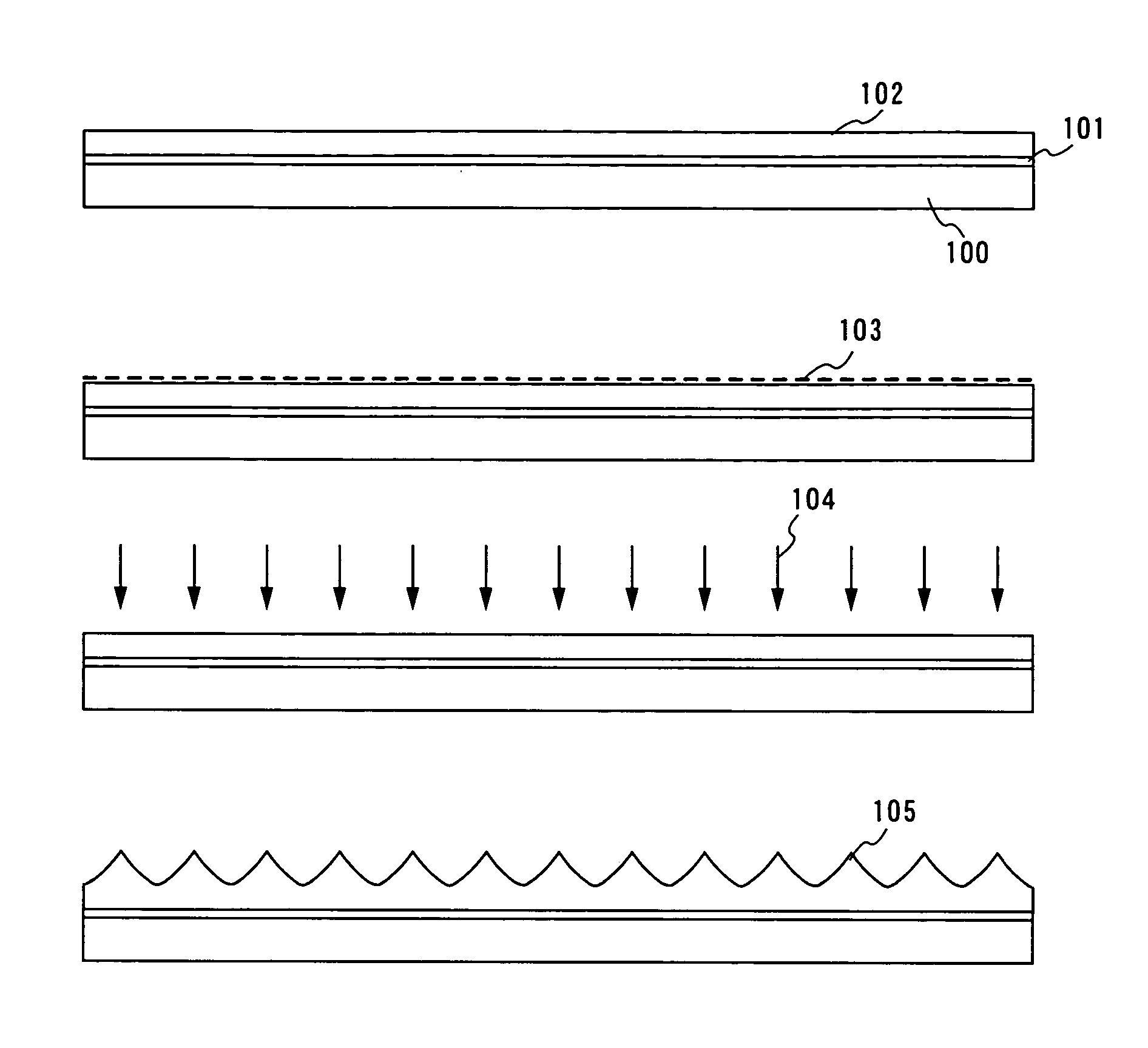
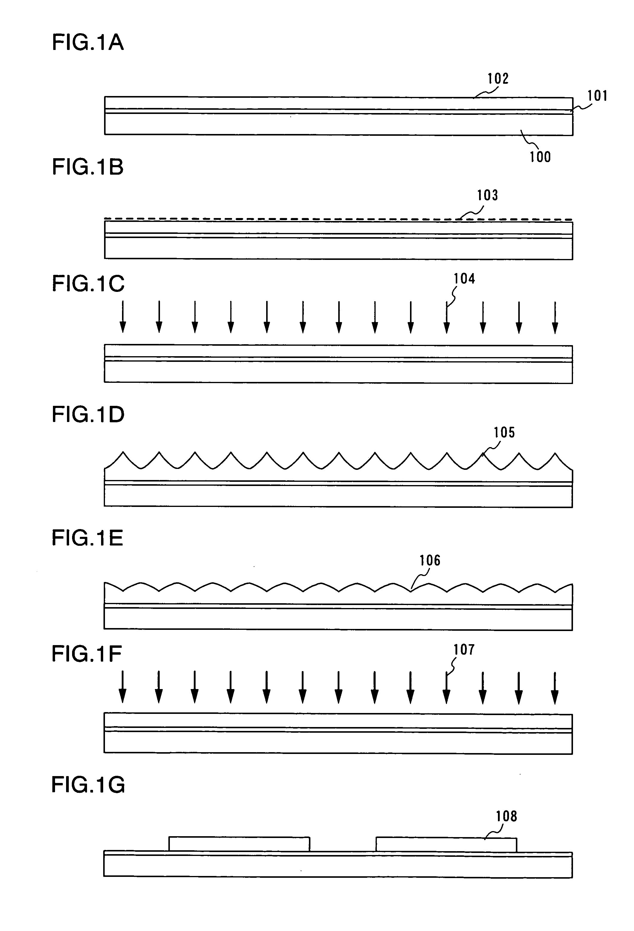
[0043]Initially, as shown in FIG. 1A, a base film 101 is formed on a substrate 100 having an insulating surface. A glass substrate such as a barium borosilicate glass or an alumino borosilicate glass, a quartz substrate, an SUS substrate, or the like can be used as the substrate 100. In addition, although the substrate made of flexible synthetic resin such as acrylic or plastic typified by PET (polyethylene terephthalate), PES (polyethersulfone), or PEN (polyethylene naphthalate) is usually inferior to the above substrates in terms of the resistance against the heat, the substrate made of flexible synthetic resin can be utilized when it can resist against the heat generated in the manufacturing steps.

[0044]The base film 101 is provided in order to prevent that alkali-earth metal or alkali metal such as Na included in the substrate 100 diffuses into the se...

embodiment mode 2

[0064]The present embodiment mode explains a method for manufacturing a crystalline semiconductor film which is different from the embodiment mode 1.

[0065]In FIG. 4A, an amorphous semiconductor film 208 having the inert element such as Ar doped is formed with the metal element segregated in the ridge and then the heat treatment is performed thereto. Before the amorphous semiconductor film 208 is formed, it is preferable to form an oxide film so that wettability is improved and that the film is not peeled. Consequently, the present embodiment mode utilizes the oxide film formed when the metal element is segregated by irradiating the laser light to the crystalline semiconductor film as shown in FIG. 1C. Therefore, the amorphous semiconductor film 208 is formed without removing the oxide film.

[0066]After that, the amorphous semiconductor film 208, the oxide film, and the ridge 105 are removed by wet etching, dry etching, or polishing with the use of the CMP (Chemical Mechanical Polishi...

embodiment mode 3

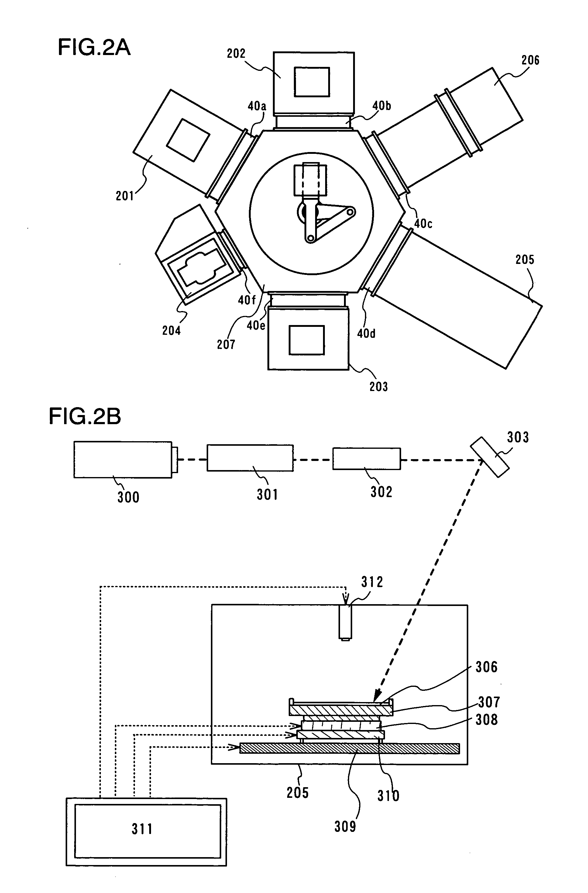
[0070]The present embodiment mode explains a multi-chamber apparatus having a laser irradiation apparatus and an optical system in the laser irradiation apparatus.

[0071]FIG. 2A shows a multi-chamber apparatus having a first treatment chamber 201 in which the processes up to forming an amorphous semiconductor film can be performed, a second treatment chamber 202 in which a metal element can be added, a third treatment chamber 203 in which a heat treatment can be performed, an unload chamber 204 for taking out a substrate, a laser irradiation chamber 205 in which the laser irradiation is performed, and a load chamber 206 in which the substrate can be stored, all of which are provided so as to encircle a transfer chamber 207. And these chambers are connected to the transfer chamber 207 with transferring gates 40a to 40f respectively interposed therebetween. As thus described, since these chambers are provided around the transfer chamber having transferring means, transportation distanc...


PUM

PropertyMeasurementUnit
widthaaaaaaaaaa
aspect ratioaaaaaaaaaa

Abstract

It is an object of the present invention to provide a method for removing the metal element from the semiconductor film which is different from the conventional gettering step for removing the metal element from the semiconductor film.In the present invention, when Ni element (Ni) is used as the metal element and a silicon-based film (referred to as a silicon film) is used as the semiconductor film, nickel silicide segregates in the ridge formed in the silicon film by irradiating the pulsed laser light. Next, etching solution of hydrofluoric acid based etchant is used to remove the nickel silicide segregated in the ridge. When the surface of the semiconductor film is rough after removing the metal element by means of etching, the laser light may be irradiated to the semiconductor film under the insert atmosphere to flatten the surface thereof.

Description

BACKGROUND OF THE INVENTION[0001]1. Field of the Invention[0002]The present invention relates to a method for manufacturing a thin film transistor having a crystalline semiconductor film manufactured by a method for reducing the concentration of a metal element included in the crystalline semiconductor film. Moreover, the present invention relates to a method for manufacturing a semiconductor device having the thin film transistor.[0003]2. Related Art[0004]Recently, a research has been advanced concerning a sophisticated semiconductor device with the use of a thin film transistor. In particular, in the semiconductor device requiring rapidity and high functionality, it is necessary to use a thin film transistor (hereinafter also referred to as TFT) having high mobility. In order to enhance the crystallinity of the semiconductor film, a crystallizing step has been performed in such a way that the metal element for promoting the crystallinity typified by nickel (Ni) is added, formed, o...

Claims


Application Information

Patent Timeline
Patent Type & Authority Patents(United States)
IPC IPC(8): H01L21/84H01L21/00H01L21/205H01L21/331H01L21/20H01L21/268H01L21/322H01L21/336H01L21/77H01L29/786
CPCH01L21/2022H01L21/268H01L21/3221H01L27/1285H01L29/78675H01L27/1277H01L29/66757H01L21/02532H01L21/02672H01L21/02686
Inventor SHIMOMURA, AKIHISAOHNUMA, HIDETOSHOJI, HIRONOBU
Owner SEMICON ENERGY LAB CO LTD
Why Eureka
Try Eureka