Method of trimming technology

a technology of photoresist layer and gate length, applied in the direction of basic electric elements, electrical equipment, semiconductor devices, etc., can solve the problems of inability to controllably print features, inability to meet the demand for sub-100 nm gate lengths for most new devices, and inability to reliably print features in photoresist layers. achieve good gate profile control

Active Publication Date: 2008-04-08
TAIWAN SEMICON MFG CO LTD
View PDF12 Cites 390 Cited by
  • Summary
  • Abstract
  • Description
  • Claims
  • Application Information

AI Technical Summary

Benefits of technology

[0018]One objective of the present invention is to provide good gate profile control during a method to trim a gate layer to afford a gate length that is smaller than can be generated by a lithography method.
[0019]A further objective of the present invention is to provide a method of trimming a gate layer where the organic masking layer has sufficient thickness to allow large scale trimming and prevents sidewall striations from forming in the trimmed gate layer.
[0020]A still further objective of the present invention is to provide a method of trimming a gate layer that does not require a hard mask to be removed after the trimming step.
[0021]Yet another objective of the present invention is to provide a trimming method that is extendable to forming gate lengths below 100 nm.

Problems solved by technology

One shortcoming of state of the art lithography processes is that they are incapable of controllably printing features such as a gate in a photoresist layer with a LG smaller than about 100 nm.
Even with the most advanced exposures tools, phase shifted masks, and other resolution enhancement techniques, the minimum feature size that can be reliably printed in a photoresist layer is not small enough to meet the demand for sub-100 nm gate lengths for most new devices.
However, the polymers in photoresists developed for 193 nm or 157 nm lithography applications in new technologies do not contain aromatic groups which have an inherently high absorbance below about 240 nm.
Therefore, the 193 nm and 157 nm photoresists based on acrylate and cyclic olefin based polymers are not as robust during a plasma etch process as their DUV (248 nm) or i-line (365 nm) predecessors which contain aromatic groups for high etch resistance.
Therefore, etching sub-100 nm features using a thin 193 nm or 157 nm based photoresist mask of about 3000 Angstroms or less that has minimal etch resistance is problematic for single layer imaging schemes.
At best, the amount of trimming or CD reduction is limited to about 10 nm or less for 193 nm or 157 nm photoresist layers which does not satisfy the need for large scale trimming of about 30 nm or more in many technologies.
However, this method also has drawbacks including a poor profile control of the hard mask and damage to the gate layer and a silicon substrate when a hardmask such as silicon nitride is removed by phosphoric acid, for example.
However, a reproducible gate length may be difficult since it depends on trimming a sloped sidewall in the bottom layer with a high degree of control.

Method used


Image

  • Method of trimming technology
  • Method of trimming technology
  • Method of trimming technology

Examples


first embodiment

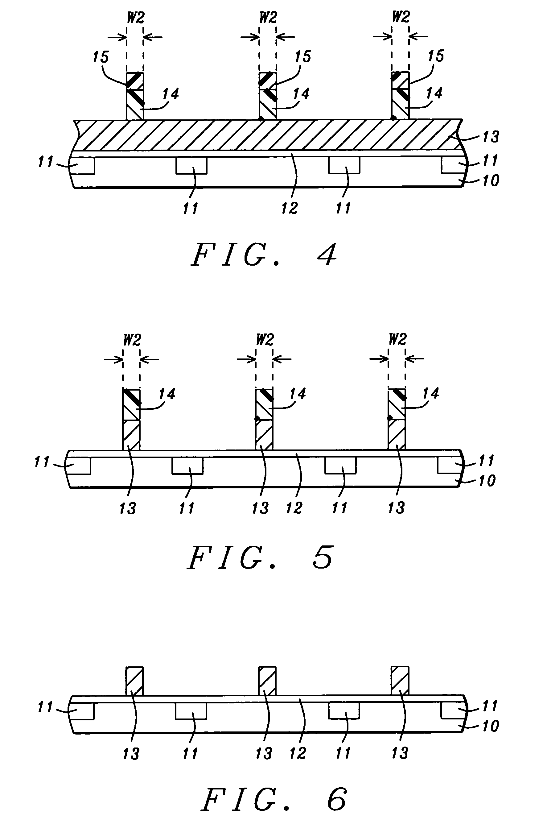
[0039]The first embodiment is depicted in FIGS. 2-6. Referring to FIG. 2, a substrate 10 is provided which is typically monocrystalline silicon but may be alternatively be based on silicon-germanium, silicon-on-insulator, or other semiconductor materials used in the art. Additionally, substrate 10 may be comprised of active and passive devices that are not shown in order to simplify the drawing. Isolation regions 11 which in the exemplary embodiment are STI regions are formed in the substrate 10 by conventional means and typically contain an insulating layer such as SiO2 or a low k dielectric material. Between adjacent isolation regions 11 is a p-well or an n-well (not shown) depending on whether a NMOS or a PMOS transistor is to be formed on an overlying active area.

[0040]A gate stack that includes a gate layer 13 on a gate dielectric layer 12 is formed on the substrate 10. First, a gate dielectric layer 12 with a thickness of about 5 to 100 Angstroms is formed on the substrate 10 ...

second embodiment

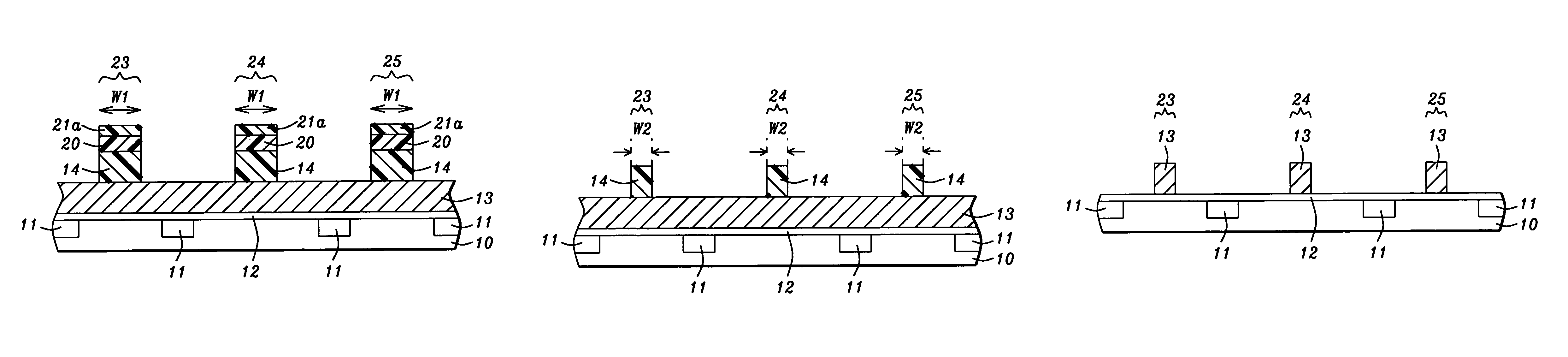
[0049]A second embodiment is illustrated in FIGS. 7-8. Referring to FIG. 7, a partially formed transistor that includes a substrate 10 with isolation regions 11, a gate dielectric layer 12, a gate layer 13, and an underlayer 14 is formed as described previously. A top photoresist layer 20 is coated to a thickness of about 500 to 5000 Angstroms. The photoresist layer 20 and underlayer 14 form a bilayer stack. The photoresist layer 20 is preferably a positive tone non-silicon containing photoresist which highly absorbs 157 nm or 193 nm radiation so that during a typical patternwise exposure, only a small portion of the photoresist layer near the surface of an exposed region undergoes a photoinduced reaction. It is understood that a post-exposure bake may be necessary to increase the rate of the photoinduced reaction in order to decrease process time. Alternatively, a shorter wavelength than 157 nm may be used such as a 13 nm wavelength from an EUV source to patternwise expose the phot...


PUM


Abstract

A process for trimming a photoresist layer during the fabrication of a gate electrode in a MOSFET is described. A bilayer stack with a top photoresist layer on a thicker organic underlayer is patternwise exposed with 193 nm or 157 nm radiation to form a feature having a width w1 in the top layer. A pattern transfer through the underlayer is performed with an anisotropic etch based on H2 / N2 and SO2 chemistry. The feature formed in the bilayer stack is trimmed by 10 nm or more to a width w2 by a HBr / O2 / Cl2 plasma etch. The pattern transfer through an underlying gate layer is performed with a third etch based on HBr / O2 / Cl2 chemistry. The underlayer is stripped by an O2 ashing with no damage to the gate electrode. Excellent profile control of the gate electrode is achieved and a larger (w1−w2) is possible than in prior art methods.

Description

FIELD OF THE INVENTION[0001]The invention relates to a method of fabricating an integrated circuit in a microelectronic device. More particularly, the present invention is directed to a method of trimming an organic layer in order to reduce a critical dimension below a feature size that can be achieved by lithographic methods.BACKGROUND OF THE INVENTION[0002]One of the key steps in the manufacture of a Metal-Oxide-Semiconductor Field Effect Transistor (MOSFET) is formation of a gate electrode comprised of a conducing layer in which a gate length is typically one of the smallest dimensions in the device. To satisfy a constant demand for higher performance devices, the gate length is continually being reduced in each successive technology generation. For current technology, a gate length (LG) as small as 60 or 70 nm is required and LG will continue to shrink as sub-100 nm technology nodes are implemented in manufacturing. One shortcoming of state of the art lithography processes is th...

Claims


Application Information

Patent Timeline
Patent Type & Authority Patents(United States)
IPC IPC(8): H01L21/3205H01L27/10H01L21/027H01L21/033H01L21/28H01L21/311H01L21/3213H01L21/336H01L21/4763H01L21/8234
CPCH01L21/0271H01L21/28123H01L21/823437H01L21/32137H01L21/32139H01L21/31138H01L21/0338
Inventor CHAN, BOR-WENHUANG, YI-CHUNPERNG, BAW-CHINGTAO, HUN-JAN
Owner TAIWAN SEMICON MFG CO LTD
Why Eureka
Try Eureka