Method of manufacturing a semiconductor device

a manufacturing method and semiconductor technology, applied in the direction of gas-filled discharge tubes, solid cathodes, radio-controlled devices, etc., can solve the problem of inability to increase the process margin, and achieve the effect of improving the decarbonization and step coverage property, reducing the dielectric constant, and improving the capacity of the interlayer insulating film

Inactive Publication Date: 2008-07-01
SEMICON ENERGY LAB CO LTD
View PDF40 Cites 19 Cited by
  • Summary
  • Abstract
  • Description
  • Claims
  • Application Information

AI Technical Summary

Benefits of technology

[0043]Because the use of organic silane including F such as FSi(OC2H5)4 instead of normal tetraethyl silicate enables SiOx of F dope small in the content of carbon and lower in dielectric constant than SiOx to be manufactured, the capacity of the interlayer insulating film between the wires in the lateral direction can be reduced. Also, in the case of using organic silane system containing carbon as a source, the present invention is very effective in improving decarbonization and the step coverage property as well as in ensuring the film forming rate.
[0044]According to the present invention, in particular, in the top-gate type thin-film transistor (TFT), after the formation of a semiconductor layer which is an active layer, the active layer is patterned, and thereafter a gate insulating film is formed. For that reason, the carbon contamination on the surface of the active layer is strong, and therefore the formation of the gate insulating film without removing it causes the reliability to be lowered with the no-good property of the transistor characteristic. Also, in the manufacture of a thin-film transistor where an oxide film having an organic silane source is formed on the gate insulating film, it is very important to obtain an oxide film which is excellent in the step coverage property, reduced in carbon and low in hygroscopicity.
[0045]In the manufacture of the semiconductor device in accordance with the present invention, the carbon impurities which could not be removed by the conventional dry ashing or wet ashing can be remarkably reduced, thereby being capable of remarkably reducing the carbon impurities in the oxide film using an organic silane source in the film. In particular, the present invention is effective in removing the impurities or the contamination including the single bond of carbon represented by C—C, thereby cleaning the interface of the semiconductor at the time of forming laminate layers of the semiconductor. Also, the present invention reduces the carbon impurities in the oxide film using the organic silane source, thereby obtaining the remarkably effects such as an improvement in the electric characteristic of the thin-film semiconductor device, an improvement in the reliability, and so on.

Problems solved by technology

Also, in cleaning due to sputtering, because damages are caused by sputtering, the effect of removing the impurities need be balanced with the damages, thereby being incapable of increasing the process margin.

Method used


Image

  • Method of manufacturing a semiconductor device
  • Method of manufacturing a semiconductor device
  • Method of manufacturing a semiconductor device

Examples


first embodiment

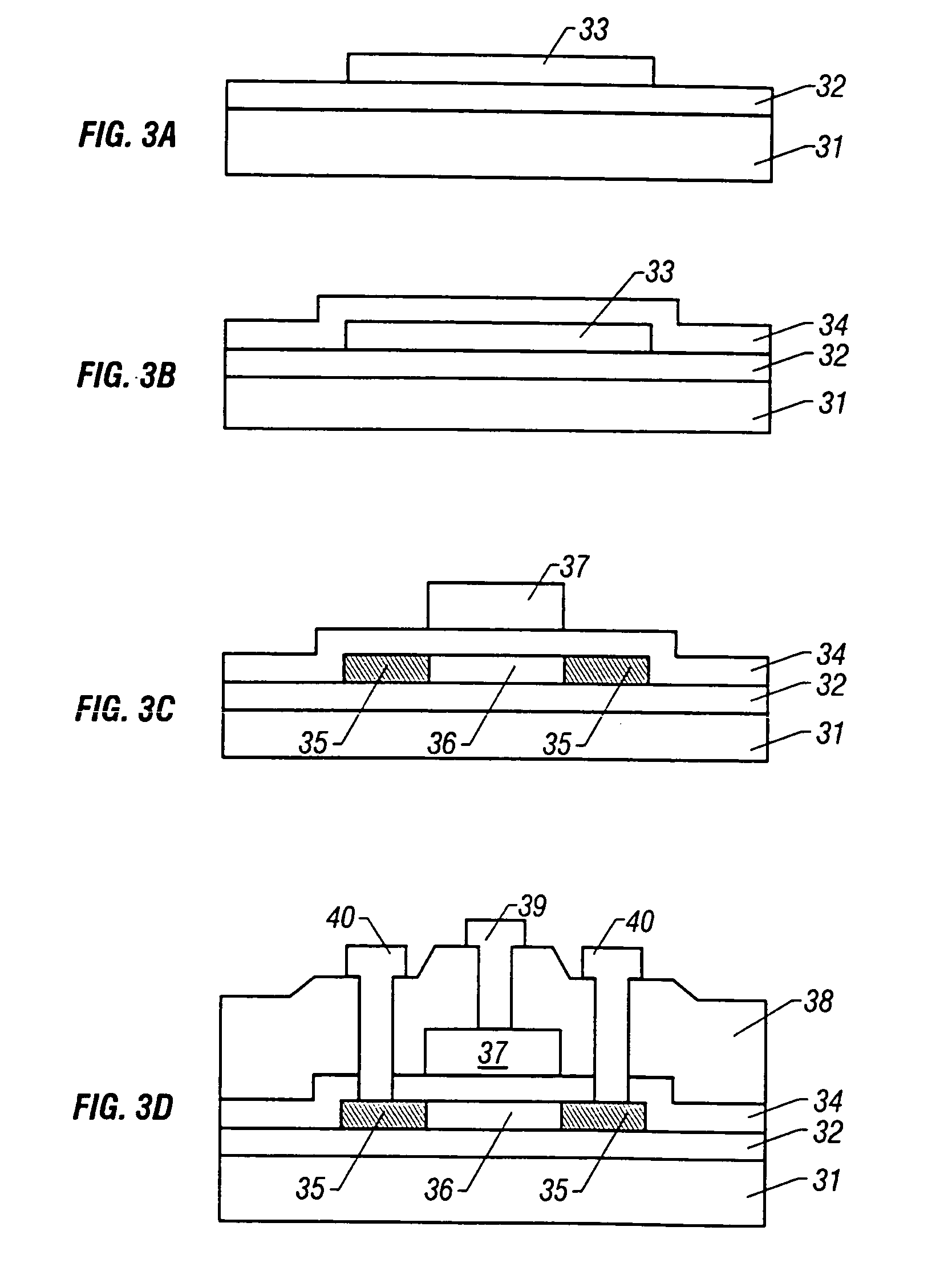
[0056]FIGS. 3A to 3D are cross-sectional views showing a process of forming a transistor in accordance with an embodiment of the present invention.

[0057]In this embodiment, the present invention is applied to a case in which a thin-film transistor is formed on a glass substrate.

[0058]On a glass substrate 31, SiO2 having a thickness of 2000 Å is used as an under film 32 through the atmospheric CVD method. Thereafter, an amorphous Si film having a thickness of 500 Å is formed as an active layer through the plasma CVD method; a resist is patterned through a known photolithography method to form a mask; the amorphous Si film is etched using CF4+O2 by dry etching; thereafter the resist is separated using an alkali separation agent to form an island 33. Then, the island 33 is allowed to grow in a solid-phase at 600° C. for 24 hours so as to change from amorphous Si to polysilicon. This is shown in FIG. 3A.

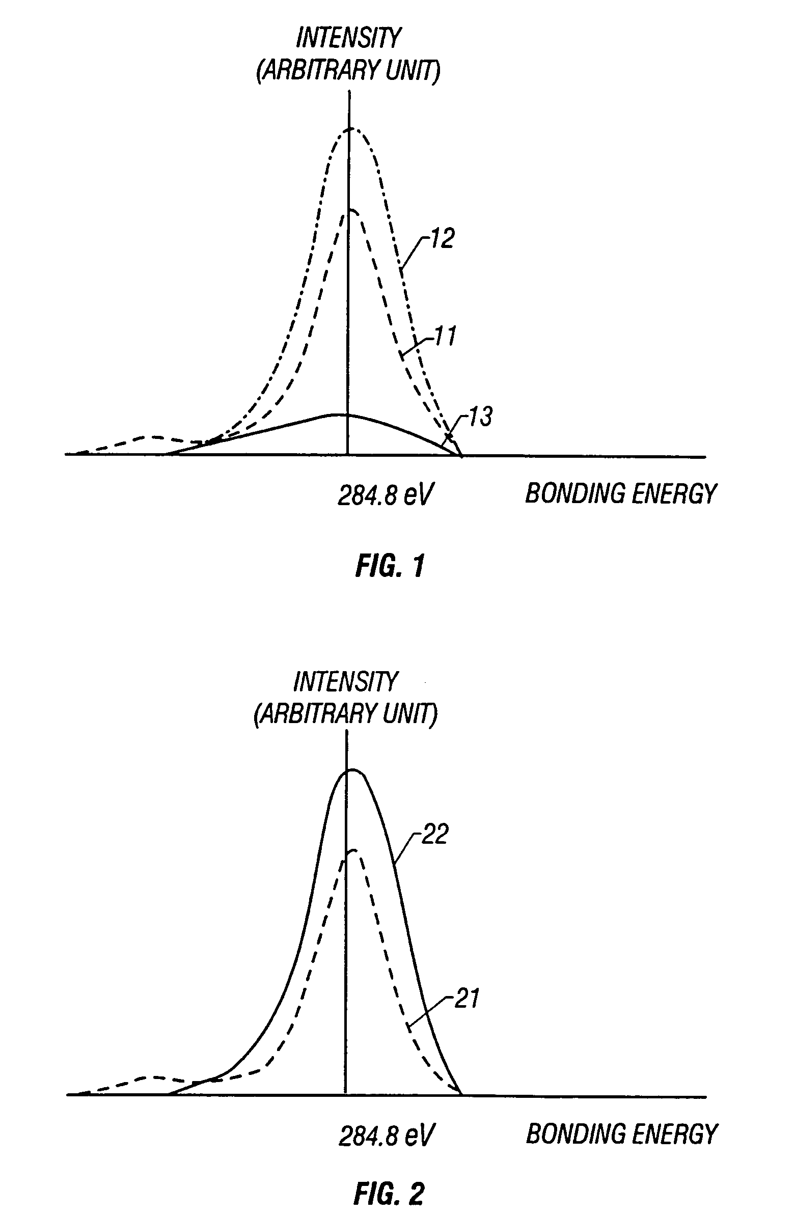
[0059]After the resist has been separated by the separation agent, the carbon contam...

second embodiment

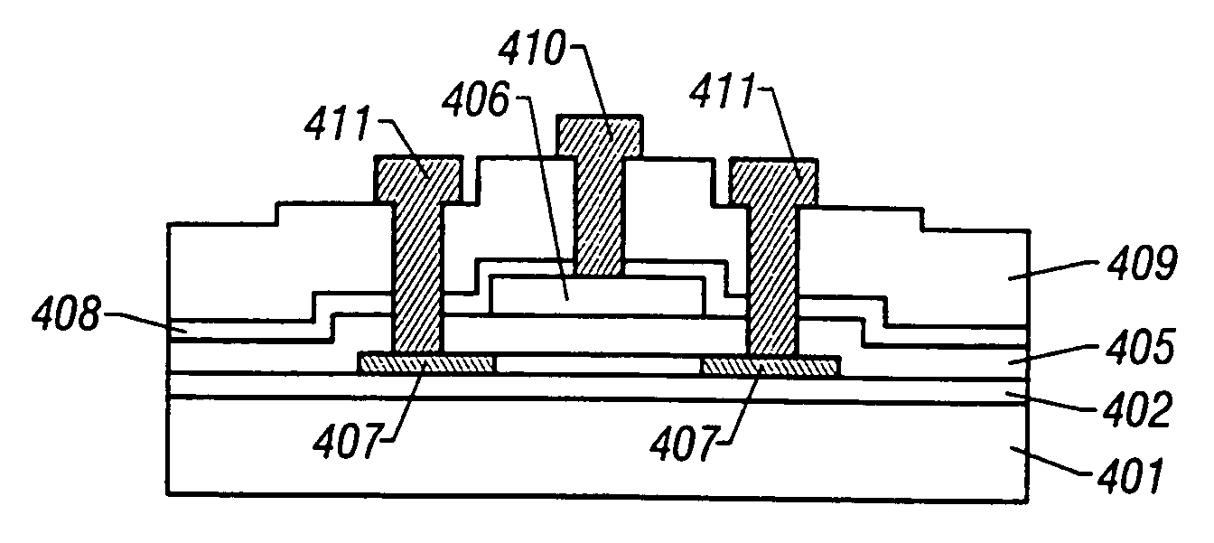
[0089]A memory in a non-volatile semiconductor storage unit is comprised of a large number of memory transistors each of which forms one basic memory transistor. The present invention is applied to the manufacture of the memory transistor. FIG. 5 is a cross-sectional view showing a basic cross-sectional structure of a memory transistor. The memory transistor is formed on a substrate 51 through the known silicon heat oxidation technique, the CVD method, the patterning of resist by the photolithography technique, and the etching technique. The memory transistor includes a polysilicon two-layer gate consisting of a tunnel oxidation film 52, a floating gate 53 made of polysilicon, an interlayer insulating film 54, and a control gate 55 made of polysilicon, a source diffusion layer 57 formed by the implantation of phosphorus or boron ions, and a drain diffusion layer 56.

[0090]The floating gate 53 is a gate for changing a threshold value of a memory transistor with respect to the control ...

third embodiment

[0105]An example in which the present invention is applied to a thin-film transistor (also called “TFT”)made of polysilicon is shown in FIG. 6. A process of forming an under film 302 on a glass substrate 301 is shown in FIG. 6A. The glass substrate 301 is made of material high in light transmission property with respect to a visual light, such as boro-silicate glass or quartz. In this embodiment, there is used Corning 7059 made by Corning Corp. In forming the under film 302, when a gate voltage is increased in an on-state direction after TFT is completed using the present invention in forming the under film 302, (for example, if the channel is of the n-channel type, the carriers flowing in the channel is electrons, and if the channel is of the p-channel type, the carriers flowing in the channel are holes.) There is a case in which a reverse-type channel occurs on the substrate 301 side below the channel.

[0106]The drain current is in principle saturated under ON state of a channel ev...


PUM


Abstract

A method of manufacturing a semiconductor device that forms laminate layers includes the steps of reducing contamination containing the single bond of carbon on at least one part of a surface on which the laminate films are formed by activated hydrogen before the laminate films are formed, and forming the laminate films on the surface on which the laminate films are formed.

Description

CROSS-REFERENCE TO RELATED APPLICATIONS[0001]This application is a divisional application of U.S. application Ser. No. 09 / 852,063, filed on May 8, 2001, now U.S. Pat. No. 6,703,264 now allowed, which is a continuation of U.S. application Ser. No. 08 / 706,667, filed on Sep. 6, 1996 (now U.S. Pat. No. 6,228,751), which claims the benefit of foreign priority applications filed in Japan as Serial No. 07-256968 on Sep. 8, 1995 and Serial No. 07-262520 on Sep. 16, 1995. This application claims priority to all of these applications, and all of these applications are incorporated by reference.BACKGROUND OF THE INVENTION[0002]1. Field of the Invention[0003]The present invention relates to a method of manufacturing, in a semiconductor device manufacturing process which is not capable of preventing a carbon contamination such as a process which is conducted within a clean room using a hopper filter, a semiconductor device providing a clean semiconductor interface with the removal of that contam...

Claims


Application Information

Patent Timeline
Patent Type & Authority Patents(United States)
IPC IPC(8): H01L21/00H01L21/336H01L29/786
CPCH01L29/66757H01L29/78612Y10S438/974
Inventor YAMAZAKI, SHUNPEISAKAMA, MITSUNORIFUKADA, TAKESHI
Owner SEMICON ENERGY LAB CO LTD
Why Eureka
Try Eureka