Nitride based LED with a p-type injection region

a technology of nitride and injection region, which is applied in the manufacture of semiconductor/solid-state devices, semiconductor devices, and semiconductor devices. it can solve the problems of reducing the internal quantum efficiency, reducing the efficiency of internal quantum efficiency, and difficulty in manufacturing a p-semiconductor layer having low resistance, so as to improve the ratio of electron-hole recombination and emission light.

Active Publication Date: 2008-09-02
SIGNIFY HLDG BV
View PDF5 Cites 73 Cited by
  • Summary
  • Abstract
  • Description
  • Claims
  • Application Information

AI Technical Summary

Benefits of technology

[0015]A semiconductor light emitting device according to the present invention includes: a semiconductor multilayer structure composed of a p-semiconductor layer, a quantum well emission layer, and an n-semiconductor layer each made of a nitride semiconductor and laminated in the stated order, light from the emission layer exiting through the n-semiconductor layer; and a p-electrode facing and in ohmic contact with the p-semiconductor layer. The p-semiconductor layer has an intensive-injection region into which an electric current from the p-electrode is injected more intensively than another region, and the intensive-injection region spans substantially across an entire surface of the p-semiconductor layer. With the stated structure, the electric current from the p-electrode is intensively injected into the p-semiconductor layer. That is to say, the current supplied to the p-electrode is injected to the p-semiconductor layer and then to the quantum well emission layer, with increased density (current density). Accordingly, the current density (carrier density) in the emission layer is increased to cause the screening effect, which cancels out the piezoelectric effect. As a result, the ratio of electron-hole recombination increases, and thus emission light increases. In addition, since the intensive-injection region spans substantially across the entire surface of the p-semiconductor layer, emission light increases substantially uniformly throughout the emission layer. Thus, light emitted by the overall emission layer increases. As a result, the luminous efficiency improves without requiring an increase of the drive current (the total amount of current injected to the emission layer).
[0016]Here, the intensive-injection region may be realized by a contact structure of the p-electrode with the semiconductor layer. In this case, the p-electrode may have, on a surface facing toward the p-semiconductor layer, a plurality of projections or depressions that are distributed substantially uniformly, and the p-electrode may be in contact with the p-semiconductor layer at a top surface thereof. With the stated structure, on supply of a drive current to the p-electrode, the current concentrates at the top surface of the p-electrode, thereby increasing its density (current density). With the increased density, the current is injected to the p-semiconductor layer and sequentially to the emission layer. Consequently, the current density (carrier density) in the emission layer is higher in a region corresponding laterally to the top surface of the p-electrode. In the corresponding region of the emission layer, the screening effect is caused to cancel the piezoelectric effect, thereby increasing the radiative recombination ratio. Since the top surface of the p-electrode spans substantially across the entire surface facing toward the p-semiconductor layer, emission light increases substantially uniformly throughout the emission layer. Thus, light emitted by the overall emission layer increases. Consequently, the luminous efficiency improves without requiring an increase of the drive current (the amount of current injected to the emission layer).
[0017]Alternatively, the intensive-injection region may be realized by a contact structure of the p-semiconductor layer with the p-electrode. In this case, the p-semiconductor layer may have, on a surface facing toward the p-electrode, a plurality of projections or depressions that are distributed uniformly, and the semiconductor multilayer structure may be in contact with the p-electrode at a top surface of the p-semiconductor layer. With the stated structure, on supply of a drive current to the p-electrode, the current is injected from the p-electrode to the semiconductor multilayer structure through the top surface of the p-semiconductor layer. Thus, the current is made to converge at the top surface of the p-semiconductor layer, thereby increasing its density (current density). With the increased density, the injected current is successively injected into the emission layer. As a result, the current density (carrier density) in the emission layer is higher in a region corresponding laterally to the top surface of the p-semiconductor layer. In the region of the emission layer, the screening effect is caused to cancel the piezoelectric effect, thereby increasing the radiative recombination ratio, and thus increasing emission light. Since the top surface of the p-semiconductor layer spans substantially across its entire surface, emission light increases substantially uniformly throughout the emission layer. Thus, light emitted by the overall emission layer increases. Consequently, the luminous efficiency improves without requiring an increase of the drive current (the amount of current injected to the emission layer).
[0018]A lighting module, a lighting device, a surface mounting device, and a display device according to the present invention each employ semiconductor light emitting devices as stated above having high luminous efficiency. Consequently, improved luminous efficiency and / or downsize of the respective modules and devices are achieved.
[0019]Furthermore, owing to its higher light efficiency, the semiconductor light emitting device produces the same level of light output with significantly less heat, in comparison with a conventional device. Consequently, the longevity of the semiconductor light emitting device is increased. Furthermore, since it is possibly to further simplify a heat dissipation mechanism, the lighting device, the surface mounting device, and the display device can be reduced both in size (thickness) and manufacturing cost.

Problems solved by technology

In the case of GaN semiconductor materials, it is generally difficult to manufacture a p-semiconductor layer having low resistance.
Unfortunately, however, GaN based LEDs have the following problem, although LEDs employing a quantum well structure exhibit improved luminous efficiency than that would otherwise be.
Existing GaN semiconductor materials suffer from piezoelectric effects generated under stress induced due to the property inherent in the materials.
The piezoelectric effects obstruct radiative recombination of electrons and holes, thereby decreasing the internal quantum efficiency.
This spatial separation of electrons and positive holes reduces the ratio of radiative recombination, thereby decreasing the luminous efficiency.
With the increase of current, however, it is inevitable that more heat is generated to elevate the temperature of LED chip.
As a result, various problems are caused, such as deterioration of property of the LED chip itself or of resin normally provided to cover the LED chip.

Method used


Image

  • Nitride based LED with a p-type injection region
  • Nitride based LED with a p-type injection region
  • Nitride based LED with a p-type injection region

Examples


embodiment 1

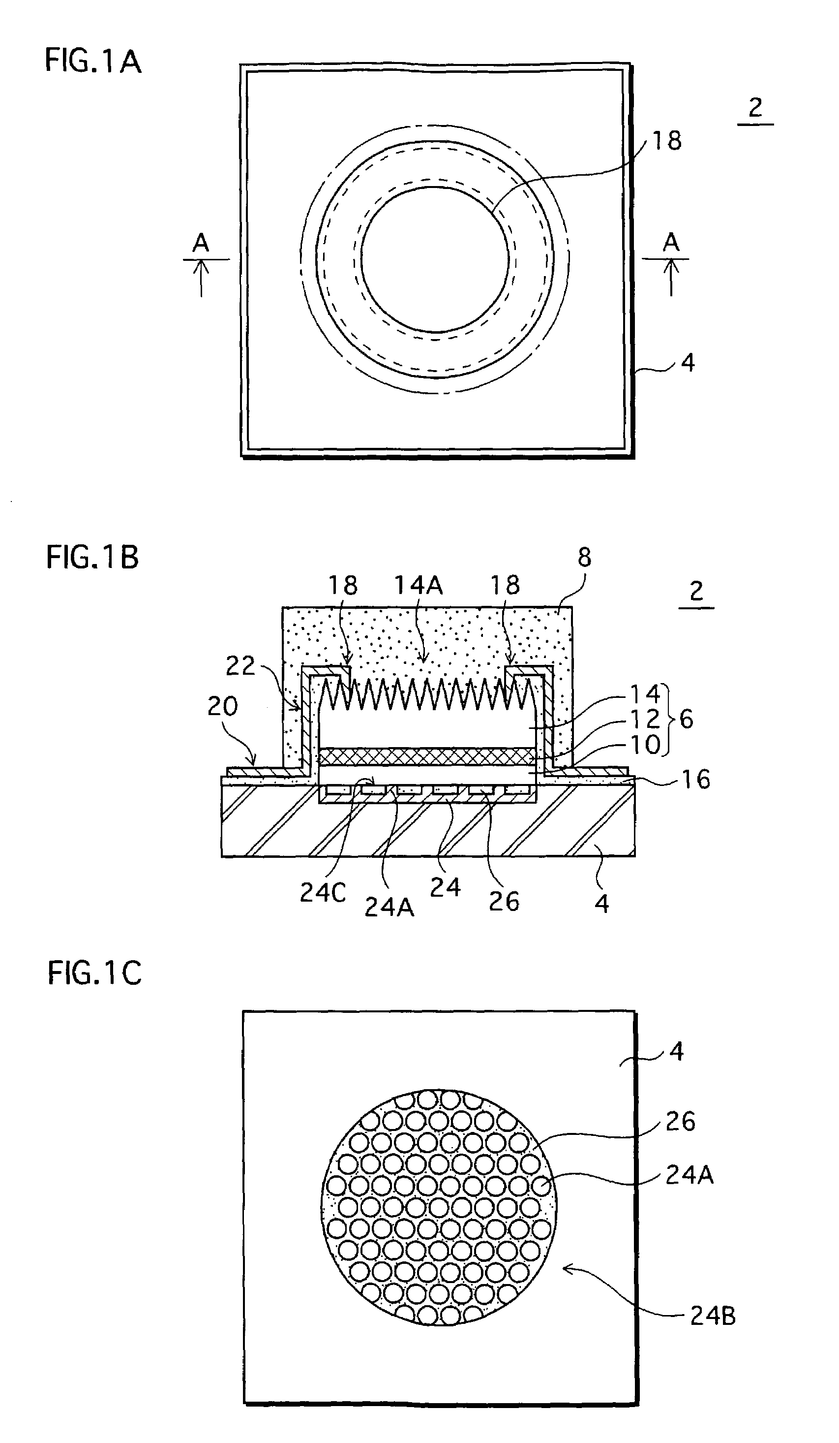
[0057]FIG. 1A is a plan view showing the schematic structure of a white LED chip 2 (hereinafter, simply “LED chip 2”), which is a semiconductor light emitting device. FIG. 1B is a sectional view taken along the line A-A of FIG. 1A. In FIG. 1A, a later-described phosphor film 8 is removed (the phosphor film 8 is shown in phantom in dot-dash lines). Note that in FIG. 1 as well as in the other figures, components are not shown on the same scale.

[0058]As shown in FIGS. 1A and 1B, the LED chip 2 is composed of: a metal substrate 4 as a base substrate; a disk-shaped (columnar) semiconductor multilayer structure 6 disposed on the metal substrate 4; and the phosphor film 8 covering the upper and side surfaces of the semiconductor multilayer structure 6. The metal substrate 4 is made of gold (Au). The dimensions of the entire LED chip 2 are as follows: the metal substrate 4 is a 500 μm square and 50 μm thick, and the phosphor film 8 is 460 μm in diameter and 200 μm in thickness.

[0059]The sem...

embodiment 2

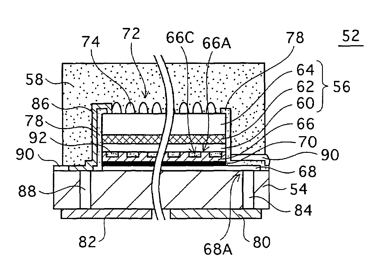
[0105]FIG. 8A is a plan view of a white LED chip 52 (hereinafter, simply “LED chip 52”), which is a semiconductor light emitting device, whereas FIG. 8B is a sectional view taken along the line B-B of FIG. 8A. FIG. 9A is a bottom view of the LED chip 52. Note that FIG. 8A shows the LED chip 52 from which a later-described phosphor film 58 (see FIG. 8B) is removed.

[0106]As shown in FIG. 8, the LED chip 52 is composed of a high-resistance Si substrate 54 (hereinafter, simply “Si substrate 54”) as a base substrate, and a semiconductor multilayer structure 56 and the phosphor film 58 laminated over the Si substrate 54. The Si substrate 54 has a main surface slightly larger than that of the semiconductor multilayer structure 56. The semiconductor multilayer structure 56 is disposed centrally on one main surface of the Si substrate 54.

[0107]The semiconductor multilayer structure 56 has a quantum well structure composed of: a p-AlGaN layer 60 (200 nm thick), which is a p-semiconductor laye...

embodiment 3

[0156]In the above embodiments 1 and 2, a semiconductor multilayer structure is initially formed on a sapphire substrate (single crystal substrate) and later bonded to a substrate of different material, such as a metal or a semiconductor. In an embodiment 3, the present invention is applied to a well-known LED chip that is manufactured by epitaxially growing a semiconductor multilayer structure on a single crystal substrate, such as an SiC substrate or sapphire substrate, and thus without involving separation of the semiconductor multilayer structure from the single crystal substrate.

[0157]FIG. 18 show an LED chip 112 according to the third embodiment. FIG. 18A is a plan view of the LED chip 112. FIG. 18B is a sectional view taking along the line C-C of FIG. 18A. FIG. 18C is a plan view exclusively of a p-electrode 126, which will be described later. Note that FIGS. 18C and 18D and FIG. 19 all show the p-electrode in plan view, and the solidly shaded areas represent the projected re...


PUM


Abstract

An LED chip (2) is composed of a p-GaN layer (10), an n-GaN layer (14), and an MQW emission layer (12) that is sandwiched between the GaN layers (10 and 14). Each layer is made of a GaN semiconductor. Light exits the LED chip (2) through the n-GaN layer (14). A p-electrode (16) of the LED chip (2) has a surface profile (24B) defined by a plurality of columnar projections (24A) formed in a uniformly distributed relation on the surface facing toward the p-GaN layer (10). The p-electrode (16) is in contact with the p-GaN layer (10) at the top surface of each projection (24A).

Description

TECHNICAL FIELD[0001]The present invention relates to a semiconductor light emitting device, a lighting module, a lighting device, a surface mounting device, and a display device. Especially, the present invention relates to a nitride semiconductor light emitting device having a quantum well emission layer.BACKGROUND ART[0002]Gallium nitride (GaN) semiconductors are III-V nitride semiconductors represented by a general formula BzAlxGa1-x-y-zInyN1-v-wAsvPw, where 0≦x≦1, 0≦y≦1, 0≦z≦1, 0≦x+y+z≦1, 0≦v≦1, 0≦w≦1, 0≦v+w≦1 (generally denoted as BA1GaInNAsP). A light emitting diode (hereinafter “LED”) is one known semiconductor light emitting device having a semiconductor multilayer structure each layer of which is made of a GaN semiconductor material. Such an LED emits light at a wide wavelength region from 200 nm to 1700 nm (from ultra-violet to infra-red), depending on the compositional ratios noted above. Especially, LEDs emitting blue light in a shorter wavelength range than blue-green ...

Claims


Application Information

Patent Timeline
Patent Type & Authority Patents(United States)
IPC IPC(8): H01L33/00H01L33/10H01L33/06H01L33/14H01L33/22H01L33/32H01L33/38H01L33/42H01L33/50H01L33/54H01L33/56H01L33/60
CPCH01L33/0079H01L33/32H01L33/385H01L33/62H01L2924/0002H01L2924/00H01L33/0093
Inventor NAGAI, HIDEO
Owner SIGNIFY HLDG BV
Why Eureka
Try Eureka