
In situ deposition of a low K dielectric layer, barrier layer, etch stop, and anti-reflective coating for damascene application

a technology of dielectric layer and damascene, which is applied in the direction of crystal growth process, instrumentation, and semiconductor/solid-state device details, etc., can solve the problems of organic arcs, increased reflections and unwanted reflections, and generally more expensive processing

Inactive Publication Date: 2008-12-30
APPLIED MATERIALS INC
View PDF377 Cites 8 Cited by
  • Summary
  • Abstract
  • Description
  • Claims
  • Application Information

AI Technical Summary

Benefits of technology

The SiC film effectively reduces capacitive coupling and reflectivity, enhancing the precision and density of integrated circuit features by providing a stable, repeatable, and multi-purpose material that can function as a barrier layer, etch stop, and anti-reflective coating, improving the throughput and reducing contamination risks in the fabrication process.

Problems solved by technology

However, typical barrier layer, etch stop, and anti-reflective coating materials have dielectric constants that are significantly greater than 7.0 that result in a combined insulator that does not significantly reduce the dielectric constant.
Thus, multi-level dielectrics and features in the damascene structures results in increased and unwanted reflections.
Organic ARCs include spin-on polyimides and polysulfones, among other materials, and are generally more expensive and require more complex processing than inorganic ARCs.
In some applications, the high κ ARC can be removed from the substrate, but the removal adds complexity to the processing sequence.
Organic ARCs can be used, but they are generally more expensive and require additional processing.
Because the values of n, k, and t are dependent on each application and each substrate thickness, the proper selection may be time consuming and onerous.
In addition, the selection of the n, k, and t values may be only applicable to narrow thickness ranges of the underlying layers which may cause additional difficulties in the repeatability of the deposition process from substrate to substrate.
Thus, the unwanted photoresist exposure from underlying layers was substantially limited to the single metal layer under the photoresist.
The dielectric layer(s) and other layers beside the conductor layers in features are comparatively transparent to the exposure light and thus more levels of reflections from multiple levels of features can hinder the photolithography processing of the upper layer.
Light reflected from the different features at different levels result in reflected light patterns back to the photoresist layer which, unless corrected, may cause unwanted exposure of the photoresist.
The capacitive coupling may lead to cross talk and / or resistance-capacitance (RC) delay, i.e., the time required to dissipate stored energy, that degrades the overall performance of the device.
But to the knowledge of the inventor, no source has adequately sought and developed a suitable ARC, barrier layer, and etch stop, using SiC.
Furthermore, no known source has found a suitable combination of chemistries that allows in situ deposition, for instance, in the same chamber, of low κ dielectric layers, and SiC barrier layers, etch stops, and ARCs.
To the knowledge of the inventor, silicon carbide that has been produced using these traditional methods has not been effective in meeting the new process requirements in low κ structures.

Method used


Image

  • In situ deposition of a low K dielectric layer, barrier layer, etch stop, and anti-reflective coating for damascene application
  • In situ deposition of a low K dielectric layer, barrier layer, etch stop, and anti-reflective coating for damascene application
  • In situ deposition of a low K dielectric layer, barrier layer, etch stop, and anti-reflective coating for damascene application

Examples


Embodiment Construction

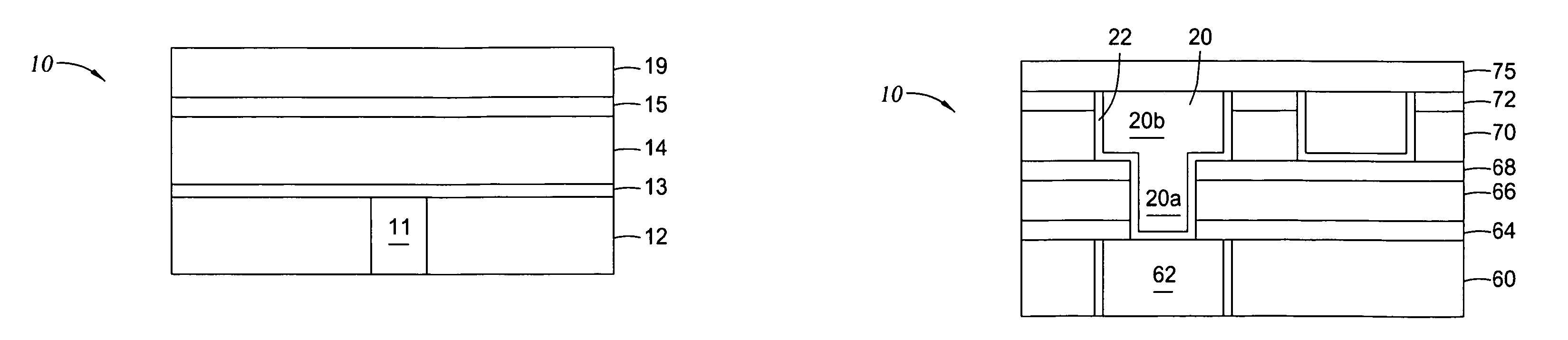
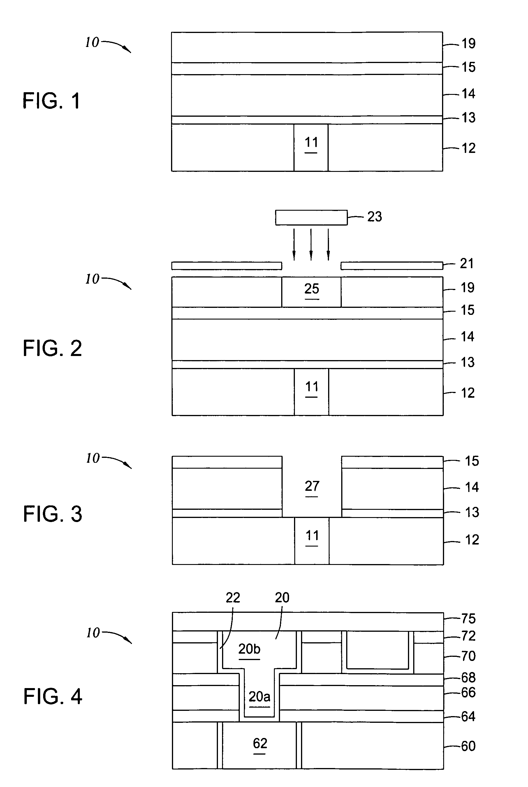
[0046]The present invention provides a SiC material, formed according to certain process regimes, useful as a barrier layer, etch stop, and / or an ARC, in multiple levels, including the pre-metal dielectric (PMD) level, in IC applications and provides a dielectric layer deposited in situ with the SiC material for the barrier layers, and etch stops, and ARCs. The dielectric layer can be deposited with different precursors as the SiC material, but preferably with the same or similar precursors as the SiC material. The present invention is particularly useful for ICs using high diffusion copper as a conductive material. The invention may also utilize a plasma containing a reducing agent, such as ammonia, to reduce any oxides that may occur, particularly on metal surfaces such as copper filled features. The invention also provides processing regimes that include using an organosilane as a silicon and carbon source, perhaps independently of any other carbon source or hydrogen source, and ...


PUM

PropertyMeasurementUnit
Reflectivityaaaaaaaaaa
spacingaaaaaaaaaa
spacingaaaaaaaaaa

Abstract

The present invention provides a SiC material, formed according to certain process regimes, useful as a barrier layer, etch stop, and / or an ARC, in multiple levels, including the pre-metal dielectric (PMD) level, in IC applications and provides a dielectric layer deposited in situ with the SiC material for the barrier layers, and etch stops, and ARCs. The dielectric layer can be deposited with different precursors as the SiC material, but preferably with the same or similar precursors as the SiC material. The present invention is particularly useful for ICs using high diffusion copper as a conductive material. The invention may also utilize a plasma containing a reducing agent, such as ammonia, to reduce any oxides that may occur, particularly on metal surfaces such as copper filled features. The invention also provides processing regimes that include using an organosilane as a silicon and carbon source, perhaps independently of any other carbon source or hydrogen source, and preferably in the absence of a substantial amount of oxygen to produce a SiC with a dielectric constant of less than 7.0. This particular SiC material is useful in complex structures, such as a damascene structure and is conducive to in situ deposition, especially when used in multiple capacities for the different layers, such as the barrier layer, the etch stop, and the ARC and can include in situ deposition of the associated dielectric layer(s).

Description

CROSS-REFERENCE TO RELATED APPLICATIONS[0001]This application is a Continuation Application of U.S. patent application Ser. No. 09 / 270,039, filed Mar. 16, 1999, now U.S. Pat. No. 6,974,766 which application is a continuation-in-part of U.S. Ser. No. 09 / 165,248, entitled “A Silicon Carbide Deposition For Use As A Barrier Layer And An Etch Stop”, filed Oct. 1, 1998, now abandoned and a continuation-in-part of U.S. Ser. No. 09 / 219,945, entitled “A Silicon Carbide Deposition For Use as a Low Dielectric Constant Anti-Reflective Coating”, filed Dec. 23, 1998, now U.S. Pat. No. 6,635,583, issued on Oct. 21, 2003, and all applications are incorporated by reference herein.FIELD OF THE INVENTION[0002]The present invention relates generally to the fabrication of integrated circuits on substrates. More particularly, the invention relates to a low temperature method for producing a low dielectric constant (low κ) silicon carbide film utilizing organosilane precursors under certain process regime...

Claims


Application Information

Patent Timeline
Patent Type & Authority Patents(United States)
IPC IPC(8): H01L21/314G03F7/11C23C16/32C23C16/42C30B25/10H01L21/027H01L21/04H01L21/205H01L21/3205H01L21/768H01L23/52H01L23/522H01L23/532H01L29/41
CPCC23C16/325H01L21/0262H01L21/0276H01L21/314H01L21/76801H01L21/76807H01L21/76829H01L21/76834H01L23/53228H01L23/53238H01L23/5329C30B25/105H01L21/02532H01L21/02381H01L21/02447C30B29/36H01L21/0445Y10S438/931Y10S438/952Y10S438/932H01L2924/0002H01L21/02274H01L21/02167H01L21/02211H01L21/02126H01L2924/00
Inventor HUANG, JUDY H.
Owner APPLIED MATERIALS INC
Features
  • Generate Ideas
  • Intellectual Property
  • Life Sciences
  • Materials
  • Tech Scout
  • Unparalleled Data Quality
  • Higher Quality Content
  • 60% Fewer Hallucinations
Learn More