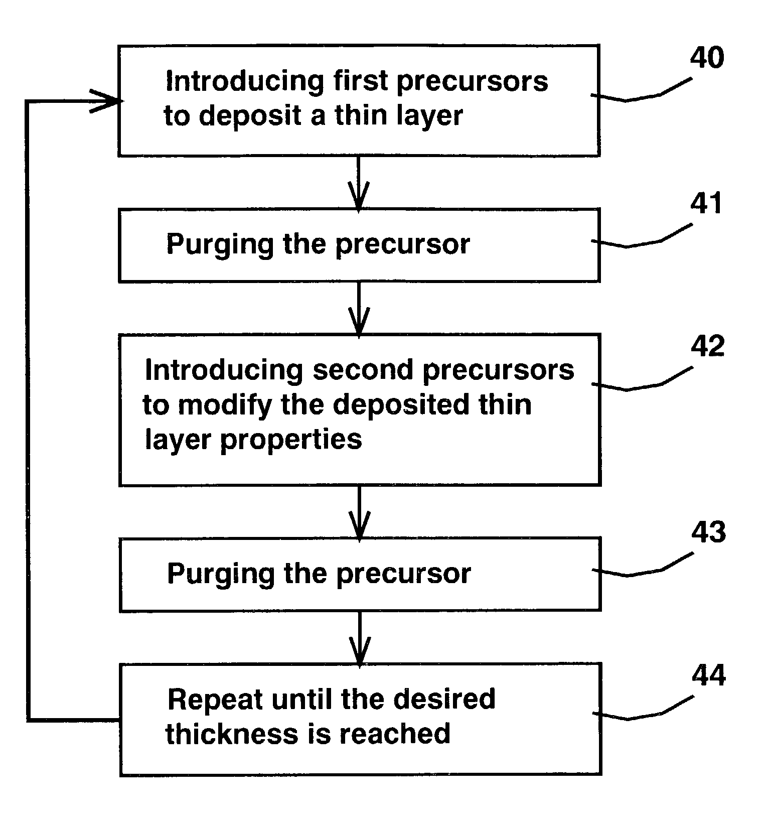
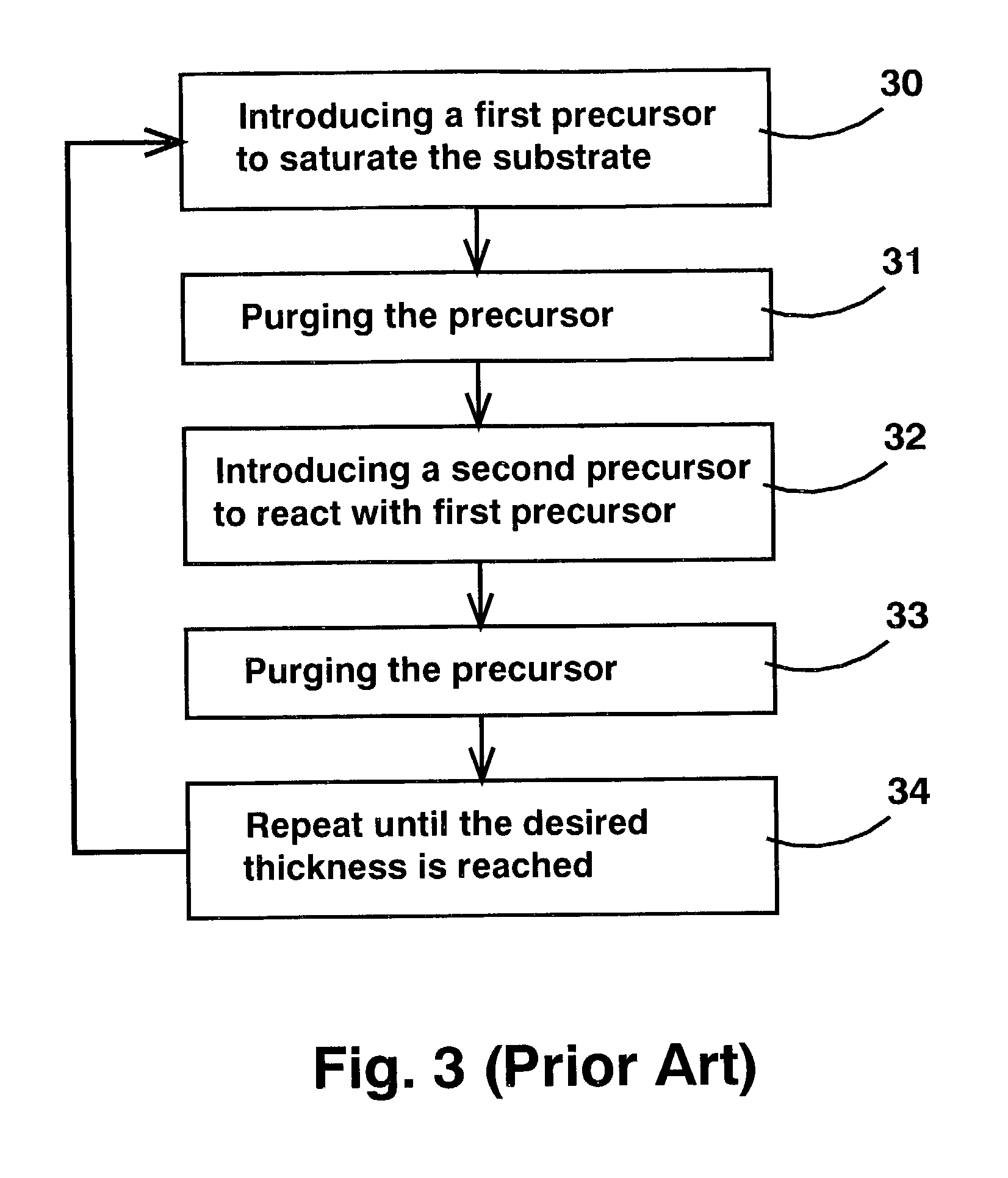
[0021]The deposition step in the present invention is not self limiting and is a function of substrate temperature and
process time. This first step is similar to a CVD process using a first set of precursors. Then the first set of precursors is turned off and purged and a second set of precursors is introduced. The purpose of the purging step is to avoid the possible interaction between the two sets of precursors. Therefore the purging can be accomplished by a pumping step to evacuate the existing precursors in the process chamber. The characteristic of the pumping step is the reduction in
chamber pressure to evacuate all gases and vapors. The purging can also be accomplished by a replacement step by using a non reacting gas such as
nitrogen or
inert gas to push all the precursors out of the process chamber. The characteristic of the replacement step is the maintaining of
chamber pressure, with the precursor turned off and the purge gas turned on. A combination of these two steps can be use in the purging step, such as a pumping step followed by a
nitrogen or
argon replacement step. The second set of precursors modifies the already deposited film characteristics. The second set of precursors can treat the deposited film such as a modification of film composition, a
doping or a removal of impurities from the deposited film. The second set of precursors can also deposit another layer on the deposited film. The additional layer can react with the existing layer to form a compound layer, or can have minimum reaction to form a nanolaminate film. The deposition step is preferably a disordered film deposition, in contrast to an ordered film deposition as in an epitaxial film. Deposition conditions for disordered film deposition are much simpler to achieve with less initial
surface preparation and less special considerations relating to the order of the deposited films. In ordered film deposition like epitaxial film deposition, small amount of precursors is typically used to allow the precursors the needed time to arrange themselves on the surface to form crystalline film. For that purpose, pulsed CVD is highly suited for epitaxial film deposition. The epitaxial deposition also requires a buffer layer to ensure a continuous lattice growth, especially with a dis-similar lattice structure of the substrate and the deposited film.
[0037]
High pressure plasma can be a little harder.
High density and
high pressure plasma require a
high energy in the chamber volume to compensate for the high collision loss due to the presence of many charged and neutral particles. To increase the power delivered to the chamber volume, an ICP power source needs to be close to the chamber volume and contains many inductive segments. These two requirements are difficult to fulfill because as the number of inductive segments increase, they are farther away from the chamber volume due to the size of the inductive segments. The inductive segments are typically a coil for the plasma source and carry a large current, therefore need to be
water cooled. Conventional inductive coil has cross section of a square or a circle with a hollow center for
water cool flow. The increase of number of inductive coil turns will increase the power, but since the successive turns are farther away from the chamber, the power increase is somewhat reduced, and at a certain distance, the power increase is no longer significant. Our plasma inductive coils is an
innovation design and has a ribbon-like cross section with the width is many times larger than the thickness. A co-pending application “
Plasma semiconductor
processing system and method” of the same authors, Ser. No. 09 / 898,439, filing date Jul. 5, 2001 has been disclosed. With the thickness of the
helical ribbon inductive coil is much less, order of mm as compared to 5 or 10 mm as conventional inductive coil, the inductive coils are much closer to the chamber volume and therefore can deliver a high power to the process chamber, resulting in a
high density,
high pressure plasma for sidewall structure treatments. The heat removal issue of the
helical ribbon is much more significant than the conventional inductive coils, but it is an
engineering issue and can be solved. With this new source of plasma, our process
chamber pressure can be as high as 1000 milliTorr, and with further improvement, can reach 5
Torr, as compared to the typical process pressure of 10 to 100 milliTorr. As a result, the sidewall treatment of our process can be very good and the result is close to 100% conformality at the sidewall and the top and bottom surface.

