Periodic plasma annealing in an ALD-type process

a plasma annealing and ald-type technology, applied in the direction of solid-state diffusion coating, crystal growth process, polycrystalline material growth, etc., can solve the problems of poor step coverage, low film conformality, high film resistivity and high impurity level, etc., to achieve low impurity level, low resistivity, and low impurity level

Active Publication Date: 2010-05-11
ASM IP HLDG BV
View PDF162 Cites 405 Cited by
  • Summary
  • Abstract
  • Description
  • Claims
  • Application Information

AI Technical Summary

Benefits of technology

[0014]Some embodiments that are described herein can achieve a level of conformality in metal and / or metal nitride films typical of thermal ALD processes in addition to low resistivity and low impurity levels typical of PEALD processes. Some embodiments improve wafer throughput by employing a relatively short plasma-on time per cycle that does not result in a negative impact on film resistivity and / or other electrical properties. Some embodiments improve the growth rate of metal films during ALD-type processes. Some embodiments reduce the susceptibility to oxidation of metals and metal precursors during ALD-type processes. Some embodiments produce better film densification than existing ALD-type processes. Some embodiments enable selective nitridation of pure metal films through periodic plasma treatment.

Problems solved by technology

Existing thermal ALD techniques can typically achieve good step-coverage deposition or conformality of metal and metal nitride films, but they can result in high film resistivity and high impurity levels.
High oxygen and halide incorporation in metal films can have a negative impact on film resistivity and / or other electrical properties, such as work function.
However, PEALD typically produces low resistivity and low impurity films at the expense of poorer step coverage relative to thermal ALD.

Method used


Image

  • Periodic plasma annealing in an ALD-type process
  • Periodic plasma annealing in an ALD-type process
  • Periodic plasma annealing in an ALD-type process

Examples


example 1

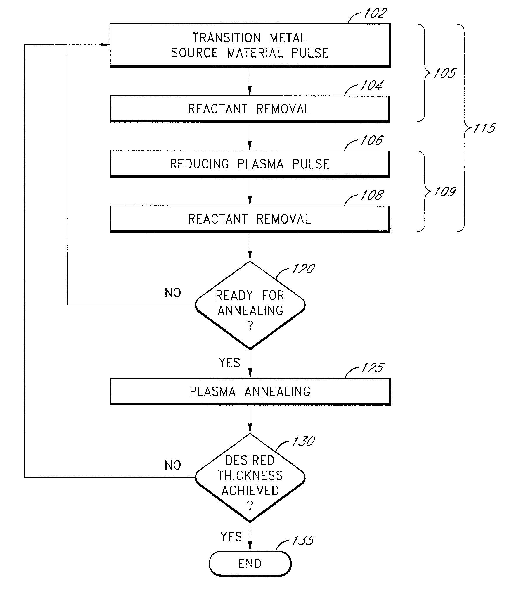
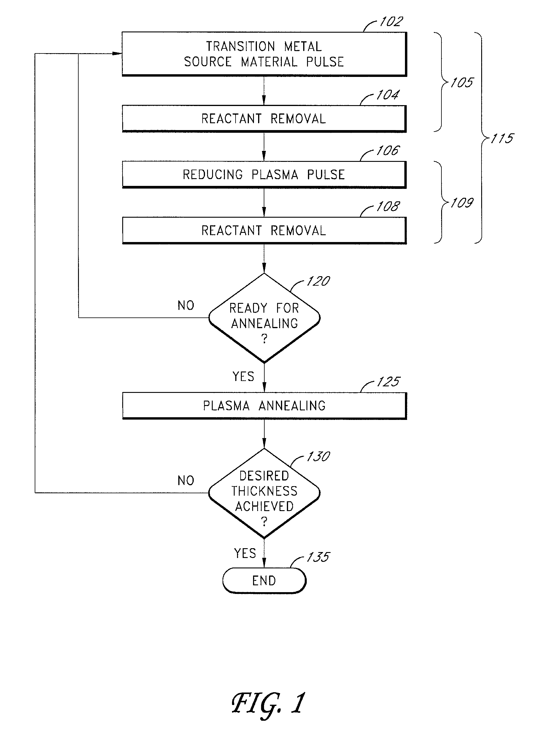
[0070]In a first example, a film including titanium is deposited in a PEALD process. The process uses a PEALD reaction chamber power of 500 W at a pressure of 2 Torr. The process includes the following steps:

[0071]1. providing a pulse of TiCl4 to the reaction space;

[0072]2. purging excess TiCl4 and reaction by-products from the reaction space with Ar for 0.65 seconds;

[0073]3. providing plasma-excited H2 to the reaction space with Ar as an inert carrier gas for 1.6 seconds;

[0074]4. purging excess plasma-excited H2 and reaction by-products from the reaction space with Ar;

[0075]5. repeating steps 1 through 4 fifty times;

[0076]6. providing plasma-excited H2 to the reaction space with Ar as an inert carrier gas for 20 seconds; and

[0077]7. repeating steps 1-6 fourteen times.

example 2

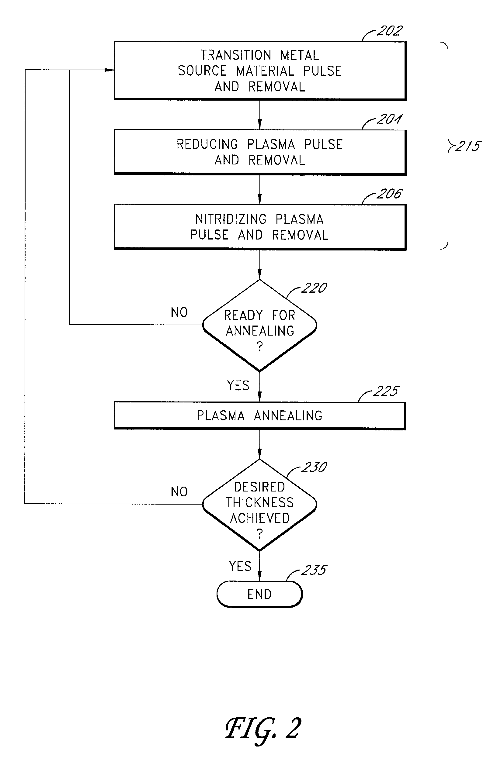
[0078]In a second example, a film including titanium nitride is deposited in a PEALD process. The process uses a PEALD reaction chamber power of 500 W at a pressure of 2 Torr. The process includes the following steps:

[0079]1. providing a pulse of TiCl4 to the reaction space;

[0080]2. purging excess TiCl4 and reaction by-products from the reaction space with Ar for 0.65 seconds;

[0081]3. providing plasma-excited H2 and plasma-excited N2 to the reaction space with Ar as an inert carrier gas for 1.6 seconds;

[0082]4. purging and / or evacuating excess plasma-excited H2, N2, and reaction by-products from the reaction space with Ar;

[0083]5. repeating steps 1 through 4 fifty times;

[0084]6. providing plasma-excited H2 and plasma-excited N2 to the reaction space with Ar as an inert carrier gas for 20 seconds; and

[0085]7. repeating steps 1-6 fourteen times.

[0086]The example process described produced a titanium nitride film with a thickness of 191 angstroms in 46 minutes. The growth rate of the l...

example 3

[0087]In a third example, a film including titanium nitride is deposited in an ALD process. The process uses a reaction chamber at a pressure of 2 Torr. The process includes the following steps:

[0088]1. providing a pulse of TiCl4 to the reaction space;

[0089]2. purging excess TiCl4 and reaction by-products from the reaction space with Ar;

[0090]3. providing NH3 to the reaction space;

[0091]4. purging excess NH3 and reaction by-products from the reaction space with Ar;

[0092]5. repeating steps 1 through 4 fifty times;

[0093]6. providing plasma-excited H2 and plasma-excited N2 to the reaction space with Ar as an inert carrier gas for 20 seconds; and

[0094]7. repeating steps 1-6 fourteen times.


PUM

PropertyMeasurementUnit
thicknessaaaaaaaaaa
thicknessaaaaaaaaaa
thicknessaaaaaaaaaa

Abstract

Methods for performing periodic plasma annealing during atomic layer deposition are provided along with structures produced by such methods. The methods include contacting a substrate with a vapor-phase pulse of a metal source chemical and one or more plasma-excited reducing species for a period of time. Periodically, the substrate is contacted with a vapor phase pulse of one or more plasma-excited reducing species for a longer period of time. The steps are repeated until a metal thin film of a desired thickness is formed over the substrate.

Description

BACKGROUND[0001]1. Field of the Disclosure[0002]The present disclosure relates to deposition of metals and metal nitride thin films. In particular, the disclosure concerns methods of using periodic plasma annealing during an atomic layer deposition process.[0003]2. Description of the Related Art[0004]The integration level of components in integrated circuits is increasing rapidly, which demands a decrease of the size of integrated circuit (IC) components and interconnects. The trend of decreasing feature size is evident, for example, in memory circuits or devices such as dynamic random access memories (DRAMs), flash memory, static random access memories (SRAMs), ferroelectric (FE) memories, and integrated circuit components, such as gate electrodes and diffusion barriers in complementary metal oxide semiconductor (CMOS) devices.[0005]Deposition methods available for forming metal and metal nitride films include atomic layer deposition (ALD), sometimes called atomic layer epitaxy (AL...

Claims


Application Information

Patent Timeline
Patent Type & Authority Patents(United States)
IPC IPC(8): H01L21/44
CPCC23C16/45542C23C16/14C23C16/56H01L21/28562C23C16/34H01L21/76843
Inventor MILLIGAN, ROBERT B.
Owner ASM IP HLDG BV
Why Eureka
Try Eureka