Mask ROM with light bit line architecture

a technology of light bit lines and mask roms, applied in the direction of transistors, digital storage, instruments, etc., can solve the problems of difficult repair of failed memory cells with redundant cells, fuse and electric fuse, and inability to change the data written on the mask rom after fabrication

Inactive Publication Date: 2010-05-11
KIM JUHAN
View PDF4 Cites 36 Cited by
  • Summary
  • Abstract
  • Description
  • Claims
  • Application Information

AI Technical Summary

Benefits of technology

[0012]In the present invention, a mask ROM with light bit line architecture is realized, wherein the mask ROM includes a capacitor as a storage element for programming with an additional contact mask during fabrication, so that the mask ROM is combined with OTP (one time programmable) memory including the same capacitor as a storage element which is programmed by breaking down after fabrication. Thereby, th...

Problems solved by technology

Thus, data written on the mask ROM cannot be changed after fabrication.
However, one drawback is that it is difficult to repair some failed memory cells with redundant cells, because the mask ROM cannot be changed after fabrication.
However, the laser fuse and electric fuse ar...

Method used


Image

  • Mask ROM with light bit line architecture
  • Mask ROM with light bit line architecture
  • Mask ROM with light bit line architecture

Examples


Embodiment Construction

)

[0035]Reference is made in detail to the preferred embodiments of the invention. While the invention is described in conjunction with the preferred embodiments, the invention is not intended to be limited by these preferred embodiments. On the contrary, the invention is intended to cover alternatives, modifications and equivalents, which may be included within the spirit and scope of the invention as defined by the appended claims. Furthermore, in the following detailed description of the invention, numerous specific details are set forth in order to provide a thorough understanding of the invention. However, as is obvious to one ordinarily skilled in the art, the invention may be practiced without these specific details. In other instances, well-known methods, procedures, components, and circuits have not been described in detail so that aspects of the invention will not be obscured.

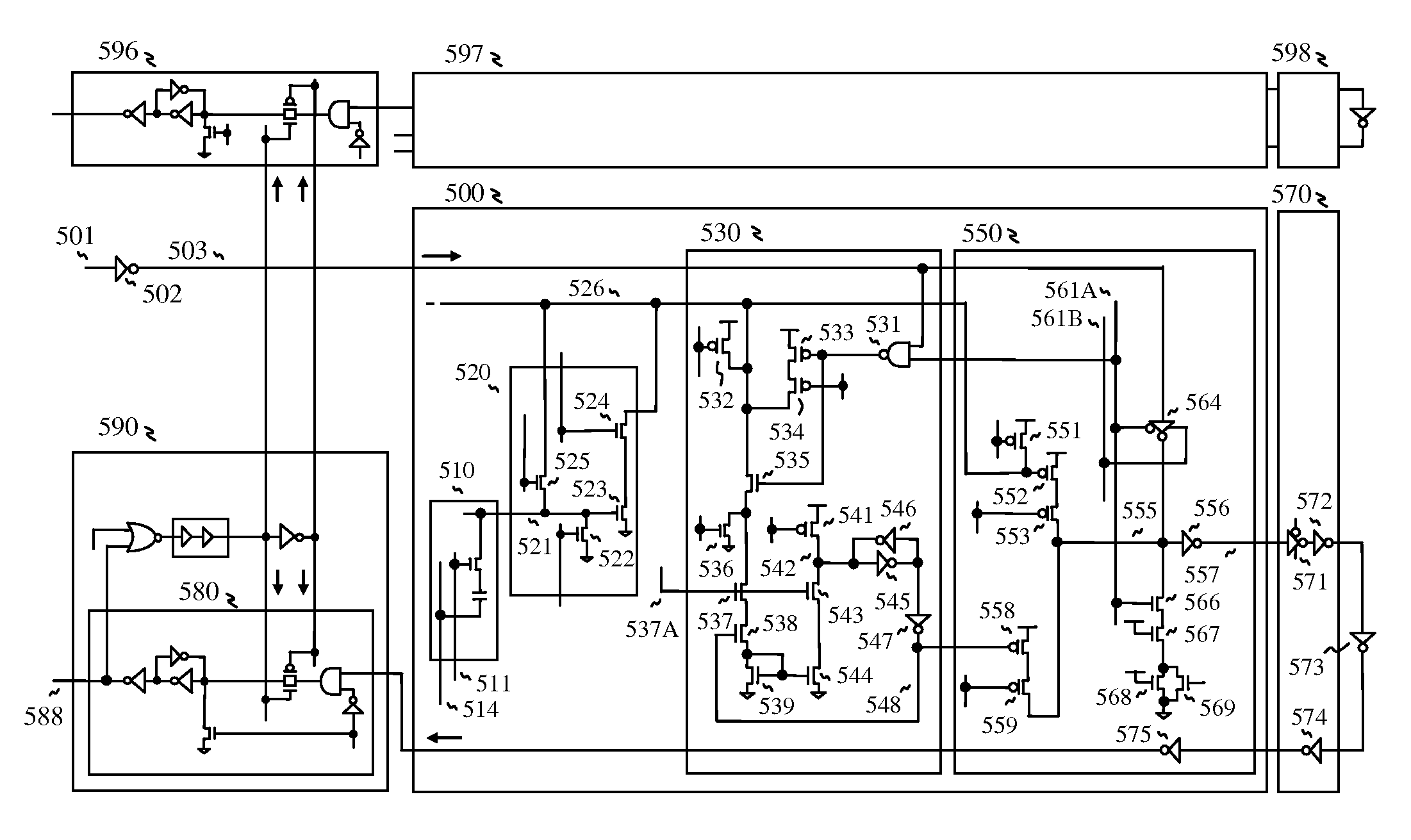
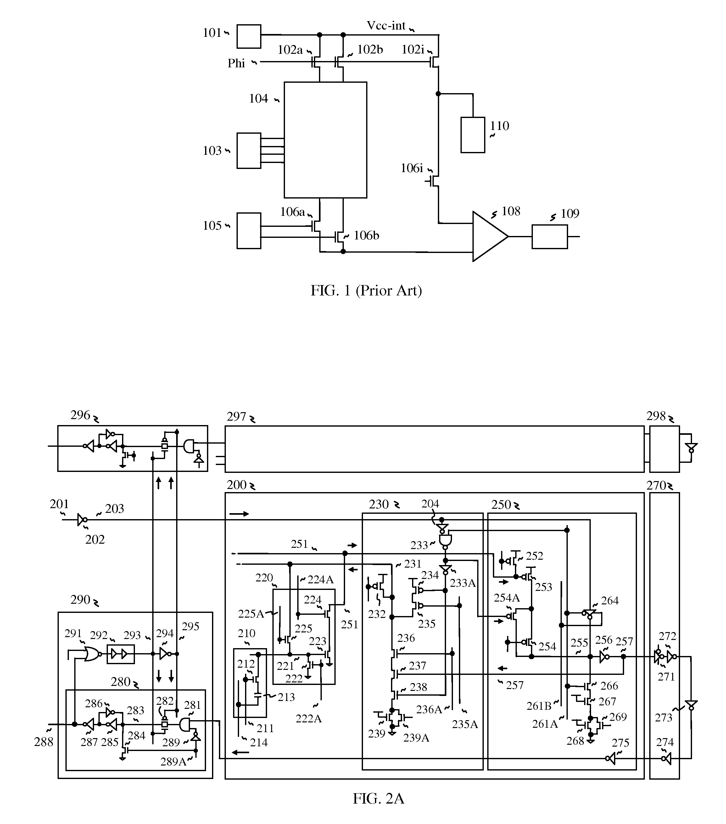
[0036]The present invention is directed to a mask ROM with light bit line architecture, as shown in...


PUM


Abstract

For improving performance of mask ROM, bit line is multi-divided for reducing capacitance, so that multi-stage sense amps are used for reading, wherein a local sense amp receives an output from a memory cell through the bit line, and a global sense amp receives the local sense amp output. By the sense amps, a voltage difference in the bit line is converted to a time difference for differentiating data “1” and data “0”. For example, data “1” is quickly transferred to an output latch circuit through the sense amps with high gain, but data “0” is rejected by a locking signal based on data “1” as a reference signal. Furthermore, a buffered data path is used for transferring data wherein the buffered data path includes a forwarding write line and a returning read line. Additionally, alternative circuits and memory cell structures for implementing the mask ROM are described.

Description

FIELD OF THE INVENTION[0001]The present invention relates to a semiconductor memory device, and more particularly, to a mask ROM (Read Only Memory) with light bit line architecture.BACKGROUND OF THE INVENTION[0002]Mask ROM is a kind of ROM (Read Only Memory) which is usually used only for reading data and is characteristically a non-volatile memory which holds contents of data even after the power is shut down. In addition, having a simple structure and high integrity, it is suitable for mass-production and cost-effective. The mask ROM is designed to provide a circuit on a semiconductor wafer using a mask on which a stored data is formed during a manufacturing process in accordance with a program indicating a user's request. Thus, data written on the mask ROM cannot be changed after fabrication.[0003]To write data on the mask ROM, there are proposed a method of causing a short-circuit between the source and drain of a memory cell by using a diffusion layer or ion implantation, and a...

Claims


Application Information

Patent Timeline
IPC IPC(8): G11C7/00
CPCG11C7/18G11C11/005G11C17/12G11C17/16G11C17/18H01L21/8221H01L27/11293H01L27/105H01L27/112H01L27/11206H01L27/11226H01L27/11286H01L27/0688H10B20/34H10B20/00H10B20/60H10B20/65H10B20/20
Inventor KIM, JUHAN
Owner KIM JUHAN
Why Eureka
Try Eureka