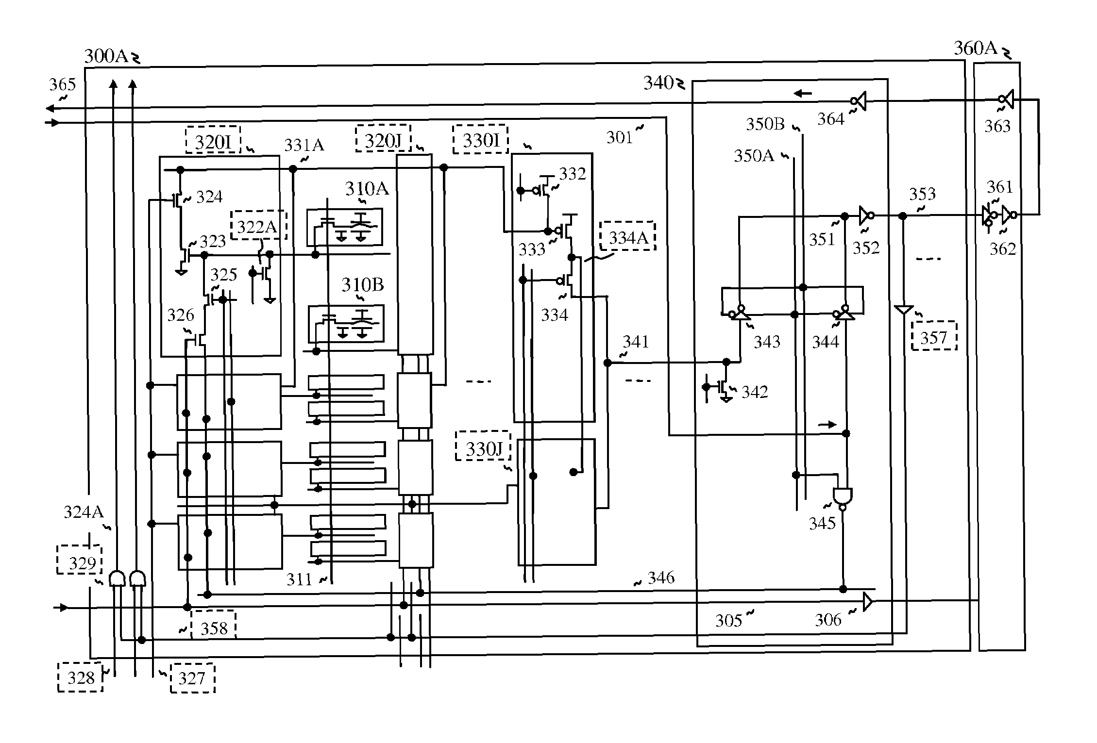
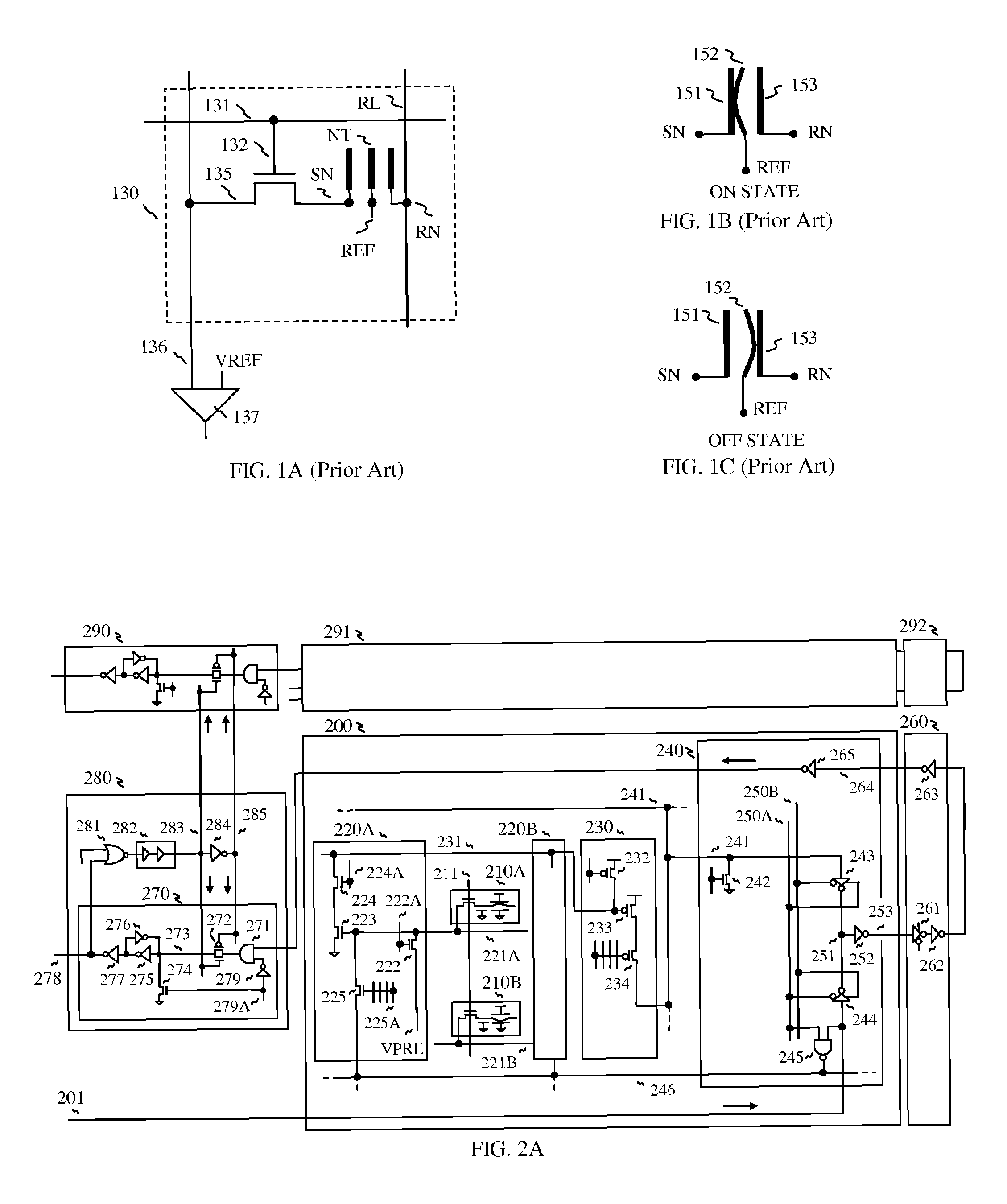
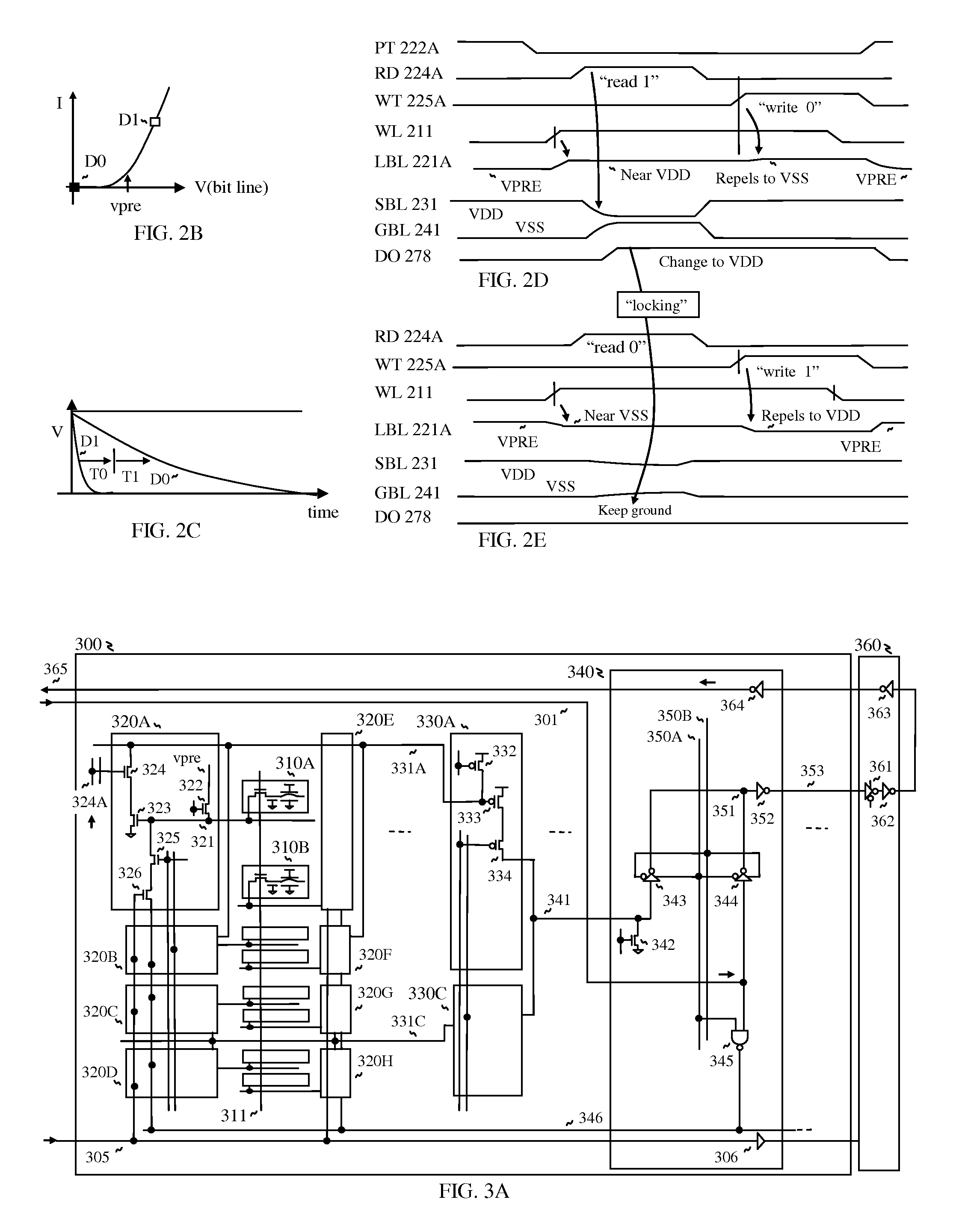
[0009]For realizing low power carbon nanotube memory, bit lines are multi-divided, so that multi-stage sense amps are used to read the memory
cell through the divided local bit lines. In particular, amplifying transistors of the sense amps are composed of relatively long channel transistors than those of pre-charge transistors in order to reduce turn-off current, which reduces operating power. Furthermore, the multi-stage sense amps are composed of dynamic circuits for eliminating static current when reading, wherein the multi-stage sense amps include a local sense amp configuring a first
dynamic circuit for reading the memory
cell through a local
bit line, a segment sense amp configuring a second dynamic circuit for reading the local sense amp through a segment bit line, and a global sense amp configuring a first tri-state
inverter for reading the segment sense amp through a global bit line, while a second tri-state inverter is used for bypassing an output from a previous
memory block, which configures a data transfer circuit with a read inverter. With multi-stage sense amp,
access time is improved because each sense amp drives lightly loaded bit lines, such that the memory
cell drives very light local bit line, the local sense amp drive the segment bit line for transferring a read output to the segment sense amp, the segment sense amp drive the global bit line for transferring the read output to the global sense amp, and the global sense amp drives a
common line of the data transfer circuit for transferring the read output to an output latch circuit.
[0011]Furthermore, configuring memory is more flexible, such that multiple memory macros can be easily configured with small segmented
memory array and multi-stage sense amps, instead of big
macro with the conventional sense amps. And number of sense amps can be determined by the target speed. For example, high speed application needs more segmented array with more sense amps, while
high density application needs more memory cells with reduced number of sense amps, thus cell efficiency is increased.
[0012]In order to match the width of the local sense amp with the memory cell, a left local sense amp is placed on the left side and a right local sense amp is placed on the right side. And the segment sense amps are also fit with two memory cells. One of prime advantages is that the local sense amp occupies small area with four transistors, and the segment sense amp is even smaller than the local sense amp with three transistors only. And write circuits are included in the local sense amp. And the global sense amp is shared by eight columns, and also output
multiplexer circuit is included in the global sense amp. As a result, the
chip area is reduced by replacing the conventional sense amp with multi-stage sense amps. In contrast, conventional architecture needs more area for adding
differential amplifier. And also the
differential amplifier occupies more space for connecting common nodes of
cross coupled transistor pairs which require a balance for matching
threshold voltage with non-minimum transistors. Furthermore, the local sense amp has high
gain with wider channel MOS transistor than that of the memory cell, and the segment sense amp has higher
gain than that of the local sense amp, which realizes fast read operation.
[0015]More specifically, a reference
signal is generated by one of fast changing data with high
gain from reference cells, which
signal serves as a reference
signal to generate a locking signal for the output latch circuit in order to reject latching another data which is slowly changed with
low gain, such that
high voltage data is arrived first while
low voltage data is arrived later, or
low voltage data is arrived first while
high voltage data is arrived later depending on configuration. The time-domain sensing scheme effectively differentiates high
voltage data and low
voltage data with time
delay control, while the conventional sensing scheme is current-domain or voltage-domain sensing scheme with a heavy bit
line pair. There are many advantages to realize the time-domain sensing scheme, so that the sensing time is easily controlled by a tunable
delay circuit, which compensates cell-to-cell variation and
wafer-to-
wafer variation, such that there is a need for adding a
delay time before locking the output latch circuit with a statistical data for all the memory cells, such as mean time between fast data and slow data. Thereby the tunable delay circuit generates a delay for optimum range of locking time. And the read output from the memory cell is transferred to the output latch circuit through a returning read path, thus the
access time is equal regardless of the location of the selected memory cell, which is advantageous to transfer the read output to the external pad at a time.
[0016]Furthermore, the current flow of the pass transistor of the memory cell can be reduced because the pass transistor only drives a lightly loaded local bit line, which means that the pass transistor can be miniaturized further. Moreover, the present invention realizes multi-stacked memory
cell structure including
thin film transistor because the memory cell only drives lightly loaded bit line even though thin film polysilicon transistor can flow lower current, for example, around 10 times lower. Thereby, bit line loading is reduced around 10 times lower for compensating the low current drivability of the pass transistor. There are almost no limits to stack multiple memory cells as long as the flatness is enough to accumulate the memory cell.
[0018]With lightly loaded bit line, cell-to-cell variation is reduced as well when reading, such that a stored voltage in the memory cell is quickly transferred to the bit line with reduced
time constant because bit line
capacitance is reduced even though
contact resistance of the suspended carbon nanotube and turn-
on resistance of a pass transistor of the memory cell are not reduced. And in order to improve read operation, a
decoupling capacitor is added to a storage node of the memory cell, which reduces gate
coupling. Without the
decoupling capacitor, the stored data may be lost when the
coupling voltage is high, because there is almost no
capacitance in the storage node of the memory cell, while the
conventional memory has enough
capacitance for
DRAM or a strong latch for SRAM. And also the
capacitor serves as a storage
capacitor for the read operation, such that the
capacitor slightly charges / discharges the bit line, when the word line is asserted. After then the carbon nanotube fully charges / discharges the bit line through one of two electrodes. Furthermore, the capacitor can reduce
soft error when alpha
ray and other rays hit the storage node.


