High speed ferroelectric random access memory

a ferroelectric random access and memory technology, applied in the field of integrated circuits, can solve the problems of slow access time, increased area, and heavy bit line loading, and achieve the effects of fast cycle operation, flexible memory configuration, and easy control of sensing tim

Inactive Publication Date: 2010-04-22
KIM JUHAN
View PDF12 Cites 36 Cited by
  • Summary
  • Abstract
  • Description
  • Claims
  • Application Information

AI Technical Summary

Benefits of technology

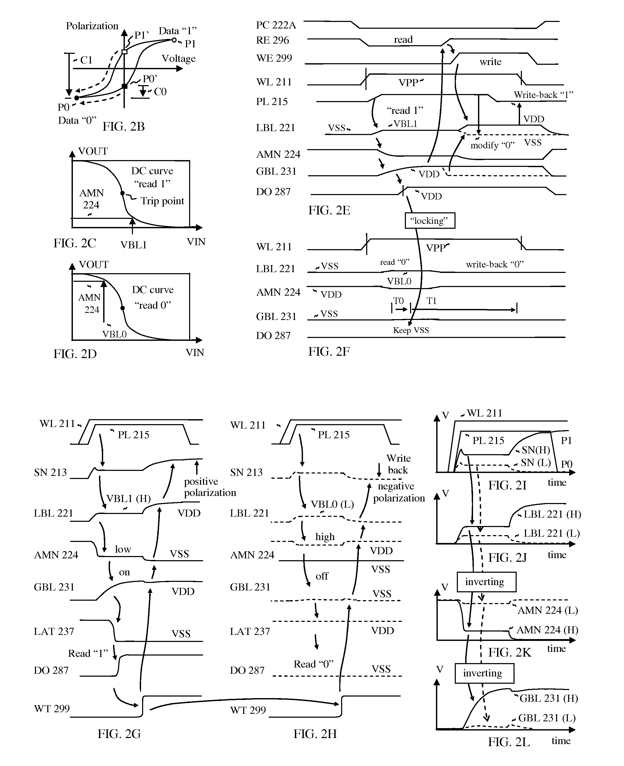
[0010]In this manner, a time domain sensing scheme is realized to differentiate data “1” and data “0”. More specifically, the reference signal is generated by one of fast changing data with high gain from reference cells, which signal serves as a reference signal to generate a locking signal in order to reject latching another data which is slowly changed with low gain, such that high capacitance data is arrived first while low capacitance data is arrived later, or low capacitance data is arrived first while high capacitance data is arrived later depending on configuration. The time domain sensing scheme effectively differentiates high capacitance data and low capacitance data with time delay control, while the conventional sensing scheme is current-domain or voltage-domain sensing scheme. In the convention memory, the selected memory cell charges or discharges the bit line, and the charged or discharged voltage of the bit line is compared by a comparator which determines an output at a time. On the contrary, in the present invention, there are many advantages to read the memory cell with time domain sensing, so that the sensing time is easily controlled by a tunable delay circuit, which compensates cell-to-cell variation and wafer-to-wafer variation, thus there is a need for adding a delay time before locking with a statistical data for all the memory cells, such as mean time between fast data and slow data. Thereby the tunable delay circuit generates a delay time for optimum range. And the read output from the memory cell is transferred to the output latch circuit through the returning read path, thus the access time is equal regardless of the location of the selected memory cell, which is advantageous to transfer the read output to the external pad at a time. And the reference signal is used for enabling the write transistor for writing back the read data or overwriting a write data, which realizes fast cycle operation.
[0011]And, configuring memory is more flexible, such that multiple memory macros can be configured with small segmented memory array and multi-stage sense amps, instead of big macro with the conventional sense amps which includes differential amps. In the present invention, number of sense amps can be determined by the target speed. For example, high speed application needs more segmented array with more sense amps, while high density application needs more memory cells with reduced number of sense amps, thus cell efficiency is increased.
[0012]And, amplifying transistors of the sense amps are composed of relatively long channel transistors than those of pre-charge transistor and reset transistor, in order to reduce turn-off current, which reduces power consumption.
[0013]And, the local sense amp has high gain with wider channel MOS transistor than that of the memory cell. Hence, the stored data in the memory cell is quickly transferred to a latch of the global sense amp. After then, the data transfer circuit transfers a read output to data output node through buffers, which realizes fast read operation with no extra waiting time.
[0015]Many alternative configurations are described, such that the ferroelectric capacitor can be used as a volatile memory when a plate line is forced to a constant voltage for eliminating fatigue of the ferroelectric capacitor as an alternative configuration, which can replace the conventional DRAM. For obtaining long retention time for the volatile memory with the constant plate line, the local bit line is pre-charged to a pre-determined voltage which is higher than ground voltage, so that sub-threshold leakage current is dramatically reduced during standby, because a word line is forced to ground voltage, which realizes a negative word line scheme without using any extra negative voltage source. More specifically, the source of the pass transistor connecting to the bit line is forced to higher than ground voltage, the word line is forced to ground voltage, and the stored charge is near supply voltage when storing data “1”. Thus, the word line voltage is lower than the voltage of the source (bit line) and the drain (storage node). In contrast, data “0” can be lost easily, but the time domain sensing scheme does not read data “0” because the locking signal rejects data “0” to be latched as explained above. Furthermore, with this sensing scheme, regular capacitor can be used for configuring the volatile memory, with regular dielectric capacitor.
[0018]And, a fingered shape capacitor is used as a storage capacitor for increasing storage capacitance in a given area, which realizes very high density memory, wherein the fingered shape capacitor is composed of a first fingered shape plate and a second fingered shape plate. And also multiple fingered shape capacitors can be formed in between metal routing layers for eliminating deep contact, where each capacitor is connected through relatively shallow contact.

Problems solved by technology

And access time is slow because there is a waiting time before the bit line is redistributed by the charges of the ferroelectric capacitor.
As a result, the area is additionally increased, because the differential amplifier occupies relatively big space.
Furthermore, the differential amplifier requires a reference voltage for comparing a voltage difference, which is one of difficult circuit with voltage and temperature variations, so that two memory cells store a data where one memory cell store positive data and another memory cell stores negative data for generating an inverted voltage reference.
However, bit line loading is still heavy, because the local bit line is connected to the global line through a transfer transistor when reading, which increases the effective capacitance of the local bit line.
And also the FRAM can replace the conventional SRAM with fixed plate line configuration for enhancing the speed as an alternative configuration, while the conventional FRAM is so slow for measuring the memory cell with changing the heavily loaded plate line.

Method used


Image

  • High speed ferroelectric random access memory
  • High speed ferroelectric random access memory
  • High speed ferroelectric random access memory

Examples


Embodiment Construction

)

[0034]Reference is made in detail to the preferred embodiments of the invention. While the invention is described in conjunction with the preferred embodiments, the invention is not intended to be limited by these preferred embodiments. On the contrary, the invention is intended to cover alternatives, modifications and equivalents, which may be included within the spirit and scope of the invention as defined by the appended claims. Furthermore, in the following detailed description of the invention, numerous specific details are set forth in order to provide a thorough understanding of the invention. However, as is obvious to one ordinarily skilled in the art, the invention may be practiced without these specific details. In other instances, well-known methods, procedures, components, and circuits have not been described in detail so that aspects of the invention will not be obscured.

[0035]The present invention is directed to high speed ferroelectric random access memory as shown i...


PUM


Abstract

For realizing high speed ferroelectric random access memory, bit line is multi-divided for reducing parasitic capacitance, so that the bit line is quickly charged or discharged by a memory cell including a ferroelectric capacitor when reading. Particularly, a non-inverting local sense amp is devised for reducing area, such that the memory cell is read by the local sense amp through a lightly loaded local bit line, and the local sense amp is read by a global sense amp through a global bit line. By the sense amps, a voltage difference in the local bit line is converted to a time difference for differentiating data “1” and data “0”, and buffered data path is used for achieving fast data transfer. Additionally, various alternative circuits and memory cell structures for implanting the memory are described.

Description

FIELD OF THE INVENTION[0001]The present invention relates generally to integrated circuits, in particular to high speed FRAM (Ferroelectric Random Access Memory).BACKGROUND OF THE INVENTION[0002]FRAM (Ferroelectric Random Access Memory) is a type of non-volatile memory device that uses such a ferroelectric capacitor and preserves stored information even when the power is off. Additionally, the FRAM has high-speed access, less power consumption, and excellent shock-resistance. Accordingly, the FRAM would be expected to be used as a main storage device for various electronic devices and equipment having file storing and retrieving functions, such as computers, networks and mobile devices.[0003]In the FRAM, a memory cell is composed of the ferroelectric capacitor and a pass transistor, and which stores logical data “1” or “0” depending on polarization state of the ferroelectric capacitor. When a voltage is applied across the ferroelectric capacitor, a ferroelectric material is polarize...

Claims


Application Information

Patent Timeline
Patent Type & Authority Applications(United States)
IPC IPC(8): G11C11/22G11C11/24G11C7/00
CPCG11C11/22G11C7/18
Inventor KIM, JUHAN
Owner KIM JUHAN
Why Eureka
Try Eureka