Semiconductor memory device

a memory device and semiconductor technology, applied in semiconductor devices, capacitors, electrical devices, etc., can solve the problems of reducing the effective storage capacitance, the dielectric film is difficult to reduce the effective oxide thickness, and the capacitors have a sufficient storage capacitance, so as to increase the relative dielectric constant of a base material made of hfo2 or zro2 and increase the oxygen coordination number of the base material

Active Publication Date: 2010-06-01
HITACHI LTD
View PDF8 Cites 16 Cited by
  • Summary
  • Abstract
  • Description
  • Claims
  • Application Information

AI Technical Summary

Benefits of technology

[0020]The present invention allows even an amorphous dielectric film to have a high relative dielectric constant. This makes it possible either to increase the amount of signal charge stored on the capacitors in DRAM and thereby enhance the operating reliability of the DRAM, or to reduce the height of these capacitors and thereby reduce the process load.
[0026]To prove this supposition, we prepared amorphous solid solutions of HfO2—La2O3, ZrO2—Y2O3, and ZrO2—La2O3 and examined their electrical characteristics. It was found that these solid solutions had a significantly reduced leakage current and an increased relative dielectric constant (30 or more), as compared to the crystalline state, as in the case of the solid solution of HfO2—Y2O3. That is, the relative dielectric constant of a base material made of HfO2 or ZrO2 can be increased by doping it with an oxide of an element having a large ion radius, such as Y2O3 or La2O3, and thereby increasing the oxygen coordination number of the base material. In this way, it is possible to provide a DRAM capacitor dielectric film that meets the 65 nm technology node.
[0027]It should be noted that the proportion of the oxide dopant is preferably 5-50%, more preferably 7-50%. If the proportion of the oxide dopant is too low, the oxygen coordination number and hence the relative dielectric constant of the base material do not increase. On the other hand, if the proportion is too high, phase separation occurs between the oxide base material and the oxide dopant, which also prevents an increase in the relative dielectric constant of the base material.
[0028]Since the capacitors in high density DRAM have a three dimensional structure, their dielectric film must be deposited by CVD, which allows for high step coverage. For example, a Y-containing organometallic material and an Hf-containing organometallic material may be introduced into an oxidizing atmosphere to form a Y2O3-doped HfO2 film; a Y-containing organometallic material and a Zr-containing organometallic material may be introduced into an oxidizing atmosphere to form a Y2O3-doped ZrO2 film; an La-containing organometallic material and an Hf-containing organometallic material may be introduced into an oxidizing atmosphere to form an La2O3-doped HfO2 film; and an La-containing organometallic material and a Zr-containing organometallic material may be introduced into an oxidizing atmosphere to form an La2O3-doped ZrO2 film.
[0031]As can be appreciated from the above description, the relative dielectric constant of a base material made of HfO2 or ZrO2 can be increased by doping it with an oxide of an element having a large ion radius, such as Y or La, and thereby increasing the oxygen coordination number of the base material. In this way, it is possible to provide a DRAM capacitor dielectric film that meets the 65 nm technology node or later.

Problems solved by technology

However, these capacitors must still store the amount of charge required for properly reading a memory to prevent soft errors.
As the minimum feature size of DRAM has been reduced, it has become increasingly difficult to ensure capacitors having a sufficient storage capacitance.
However, the MIS structure is disadvantageous in that it is difficult to reduce the EOT (Effective Oxide Thickness) of the dielectric film, since an SiO2 layer grows at the interface between the lower electrode and the dielectric film during formation of the film and during the postheat treatment and reduces the effective storage capacitance.
However, it is not easy to implement such a dielectric film forming method.
That is, there are no capacitor dielectric materials currently available that meet the 65 nm-technology node.
That is, if the dielectric material has a larger free energy of oxide formation than TiO2 (for example, if it is Ta2O5), the dielectric film (or material) oxidizes the TiN electrodes, resulting in reduced effective capacitance and / or increased leakage current.

Method used


Image

  • Semiconductor memory device
  • Semiconductor memory device
  • Semiconductor memory device

Examples


first embodiment

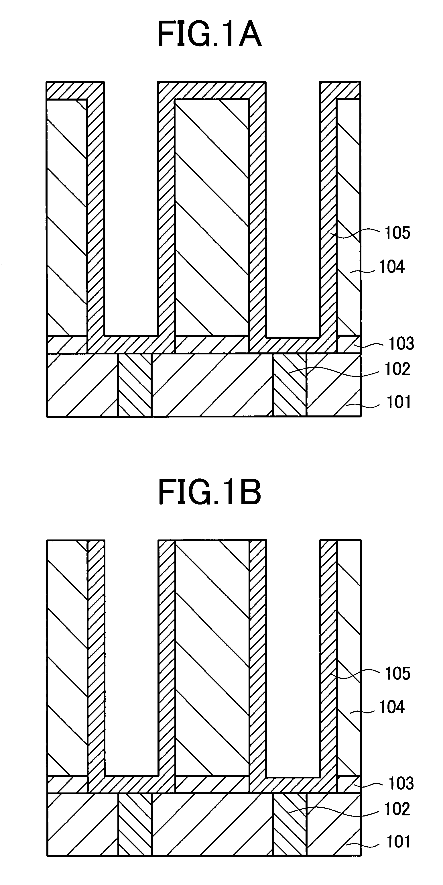
[0038]A first embodiment of the present invention will be described with reference to FIGS. 1A to 1D. These figures are cross-sectional views showing an MIM capacitor structure that employs a dielectric film doped with an element having a large ion radius. For example, this MIM capacitor structure can be applied to semiconductor memory devices, especially DRAM.

[0039]First, the steps before and including the step of forming the lower electrode will be described with reference to FIGS. 1A and 1B. Referring to FIG. 1A, plugs 102 of polysilicon are formed in a plug section interlayer insulating film 101 made up of a silicon oxide film. The plugs 102 are provided to electrically connect between the memory cell select transistor and the capacitor.

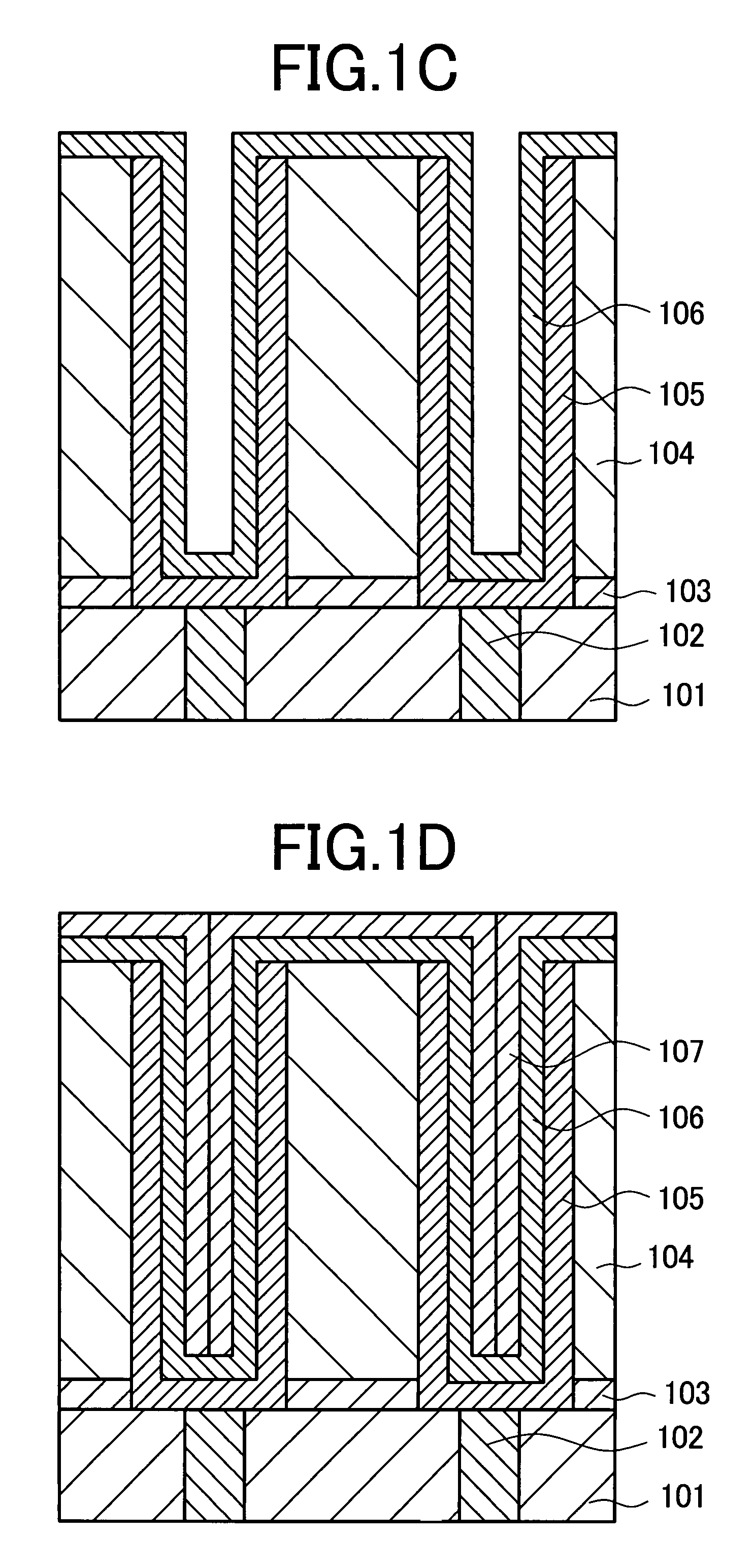
[0040]Then, a silicon nitride film 103 and a capacitor section interlayer insulating film 104 made up of a silicon oxide film are deposited, and trenches are formed in these films so as to expose the plugs 102. The capacitor section interlayer in...

second embodiment

[0049]A second embodiment of the present invention will be described with reference to FIGS. 2A to 2D. These figures are cross-sectional views showing an MIM capacitor structure that employs a dielectric film doped with an element having a large ion radius. For example, this MIM capacitor structure can be applied to semiconductor memory devices, especially DRAM. It should be noted that the MIM capacitor structure of the present embodiment differs from that of the first embodiment in that portions of the outer sidewalls of the lower electrode are used to form capacitance.

[0050]First, the steps before and including the step of forming the lower electrode will be described with reference to FIGS. 2A and 2B. Referring to FIG. 2A, plugs 102 of polysilicon are formed in a plug section interlayer insulating film 101 made up of a silicon oxide film. The plugs 102 are provided to electrically connect between the memory cell select transistor and the capacitor.

[0051]Then, the following films ...

third embodiment

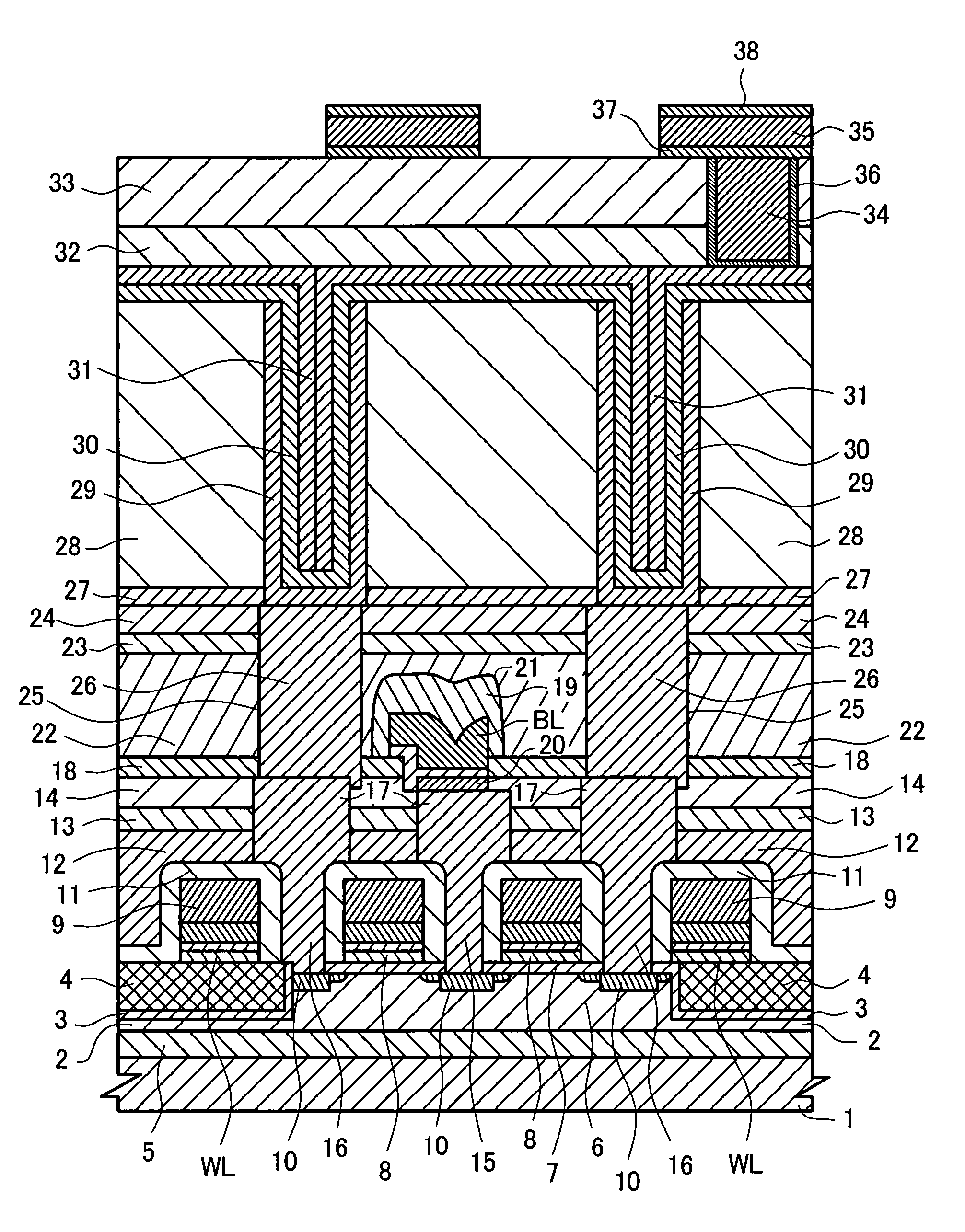
[0058]A third embodiment of the present invention will be described with reference to FIG. 3. The third embodiment provides a DRAM employing the MIM capacitor structure of the first embodiment.

[0059]There will be described a method for manufacturing this DRAM.

[0060]FIG. 3 is a cross-sectional view of the DRAM employing an MIM capacitor structure according to the present embodiment. First, trench isolation regions 4 and an impurity-doped P-type well 6 are formed in the semiconductor substrate 1 in the following manner. First, a P-type single-crystal silicon semiconductor substrate 1 having a specific resistance of approximately 10 Ocm is provided. Then, a thin silicon oxide film (now shown) having a thickness of approximately 10 nm and a silicon nitride film (not shown) having a thickness of approximately 140 nm are formed over the semiconductor substrate 1. More specifically, the silicon oxide film is formed by wet oxidation, e.g., at approximately 850° C., and the silicon nitride f...


PUM


Abstract

HfO2 films and ZrO2 films are currently being developed for use as capacitor dielectric films in 85 nm technology node DRAM. However, these films will be difficult to use in 65 nm technology node or later DRAM, since they have a relative dielectric constant of only 20-25. The dielectric constant of such films may be increased by stabilizing their cubic phase. However, this results in an increase in the leakage current along the crystal grain boundaries, which makes it difficult to use these films as capacitor dielectric films. To overcome this problem, the present invention dopes a base material of HfO2 or ZrO2 with an oxide of an element having a large ion radius, such as Y or La, to increase the oxygen coordination number of the base material and thereby increase its relative dielectric constant to 30 or higher even when the base material is in its amorphous state. Thus, the present invention provides dielectric films that can be used to form DRAM capacitors that meet the 65 nm technology node or later.

Description

CLAIM OF PRIORITY[0001]The present application claims priority from Japanese application JP 2006-091842 filed on Mar. 29, 2006, the content of which is hereby incorporated by reference into this application.BACKGROUND OF THE INVENTION[0002]1. Field of the Invention[0003]The present invention relates to semiconductor devices and manufacturing methods therefore, and more particularly relates to a technique that can be advantageously applied to semiconductor devices employing capacitors, such as dynamic random access memory (DRAM), and to manufacturing methods therefore.[0004]2. Description of the Related Art[0005]Increasing the integration density of a semiconductor device including an LSI, such as DRAM, requires reducing the size of the capacitors in the device. However, these capacitors must still store the amount of charge required for properly reading a memory to prevent soft errors. That is, in order to enhance the integration density of a semiconductor device (such as DRAM), it ...

Claims


Application Information

Patent Timeline
Patent Type & Authority Patents(United States)
IPC IPC(8): H01L27/108H01L29/94
CPCH01L27/10852H01L21/31641H01L21/31645H01L28/91H01L27/10894H01L27/10814H01L21/02271H01L21/022H01L21/02175H10B12/315H10B12/09H10B12/033H10B12/00
Inventor MATSUI, YUICHIMIKI, HIROSHI
Owner HITACHI LTD
Why Eureka
Try Eureka